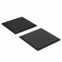
LH7A400N0G000B5;55 NXP Semiconductors, LH7A400N0G000B5;55 Datasheet - Page 12

LH7A400N0G000B5;55
Manufacturer Part Number
LH7A400N0G000B5;55
Description
IC ARM9 BLUESTREAK MCU 256BGA
Manufacturer
NXP Semiconductors
Series
BlueStreak ; LH7Ar
Datasheet
1.LH7A400N0F000B555.pdf
(65 pages)
Specifications of LH7A400N0G000B5;55
Core Size
16/32-Bit
Core Processor
ARM9
Speed
200MHz
Connectivity
EBI/EMI, IrDA, Microwire, MMC, SmartCard, SPI, SSI, SSP, UART/USART, USB
Peripherals
AC'97, DMA, LCD, POR, PWM, WDT
Number Of I /o
60
Program Memory Type
ROMless
Ram Size
80K x 8
Voltage - Supply (vcc/vdd)
1.71 V ~ 3.6 V
Oscillator Type
External
Operating Temperature
-40°C ~ 85°C
Package / Case
256-BGA
Controller Family/series
(ARM9)
No. Of I/o's
60
Ram Memory Size
80KB
Cpu Speed
200MHz
No. Of Timers
3
No. Of Pwm Channels
2
Digital Ic Case Style
BGA
Processor Series
LH7A4
Core
ARM9TDMI
Data Bus Width
32 bit
Mounting Style
SMD/SMT
3rd Party Development Tools
MDK-ARM, RL-ARM, ULINK2
Lead Free Status / RoHS Status
Lead free / RoHS Compliant
Eeprom Size
-
Program Memory Size
-
Data Converters
-
Lead Free Status / Rohs Status
Details
Other names
568-4334
935285038557
935285038557
LH7A400
1. Signals beginning with ‘n’ are Active LOW.
2. The SCLK pin can source up to 12 mA and sink up to 20 mA. See ‘DC Characteristics’.
3. Schmitt trigger input; see ’DC Specifications’, page 31 for triggers points and hysteresis.
4. Input only for JTAG boundary scan mode.
5. Output only for JTAG boundary scan mode.
6. The internal pullup and pull-down resistance on all digital I/O pins is 50 k
7. When used as SMBCLK, this pin must have a resistor.
8. The RESET STATE is defined as the state during power-on reset.
9. The STANDBY STATE is defined as the state when the device is in standby. During this state,
10. All unused USB Device pins with a differential pair must be pulled
12
BGA
R12
R15
P11
T12
PIN
G1
G2
G4
G5
H1
H2
H3
C3
D1
D2
A1
B1
B2
C1
F6
F5
I/O cells are forced to input (Input), output driving low (LOW), output driving high (HIGH), or their
current state is preserved (No Change). In some case, function selection has an overall effect on the standby state.
to ground with a 15 k
Normal
MODE
JTAG
LFBGA
T14
T15
P15
P13
PIN
G2
G1
H3
H5
H6
H7
H2
H1
C2
D3
C1
F5
E3
F6
E5
J1
Table 4. nTest Pin Function
nTEST0
COL0
COL1
COL2
COL3
COL4
COL5
COL6
COL7
TBUZ
MEDCHG
WIDTH0
WIDTH1
BATOK
nBATCHG
TDI
TCK
TDO
TMS
nTEST0
nTEST1
0
1
SIGNAL
Ω
resistor.
nTEST1
Keyboard Interface
Timer Buzzer (254 kHz MAX.)
Boot Device Media Change. Used with WIDTH0
and WIDTH1 to specify boot memory device.
External Memory Width Pins. Also, used with
MEDCHG to specify the boot memory device size.
The pins must be pulled HIGH with a 33 kΩ resistor.
Battery OK
Battery Change
JTAG Data In. This signal is internally pulled-up t
o VDD.
JTAG Clock. This signal should be externally
pulled-up to VDD with a 33 kΩ resistor.
JTAG Data Out. This signal should be externally
pulled up to VDD with a 33 kΩ resistor.
JTAG Test Mode select. This signal is internally
pulled-up to VDD.
Test Pin 0. Internally pulled up to VDD. For Normal
mode, leave open. For JTAG mode, tie to GND.
See Table 4.
Test Pin 1. internally pulled up to VDD. For Normal
and JTAG mode, leave open. See Table 4.
1
1
Table 3. Functional Pin List (Cont’d)
nURESET
DESCRIPTION
Rev. 01 — 16 July 2007
1
x
NXP Semiconductors
Ω
RESET
STATE
High-Z
HIGH
LOW
Input
Input
Input
Input
Input
Input
Input
Input
No Change
No Change
No Change
No Change
No Change
No Change
No Change
No Change
No Change
STANDBY
STATE
HIGH
LOW
32-Bit System-on-Chip
Preliminary data sheet
OUTPUT
DRIVE
8 mA
8 mA
4 mA
I/O NOTES
O
O
O
I
I
I
I
I
I
I
I
3
3
3
3
4
3
4
4


