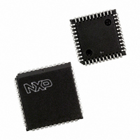
P89LV51RD2FA,512 NXP Semiconductors, P89LV51RD2FA,512 Datasheet - Page 63

P89LV51RD2FA,512
Manufacturer Part Number
P89LV51RD2FA,512
Description
IC 80C51 MCU 1024 RAM 44PLCC
Manufacturer
NXP Semiconductors
Series
89LVr
Datasheet
1.P89LV51RD2BBC557.pdf
(76 pages)
Specifications of P89LV51RD2FA,512
Core Processor
8051
Core Size
8-Bit
Speed
33MHz
Connectivity
SPI, UART/USART
Peripherals
Brown-out Detect/Reset, POR, PWM, WDT
Number Of I /o
32
Program Memory Size
64KB (64K x 8)
Program Memory Type
FLASH
Ram Size
1K x 8
Voltage - Supply (vcc/vdd)
2.7 V ~ 3.6 V
Oscillator Type
Internal
Operating Temperature
-40°C ~ 85°C
Package / Case
44-PLCC
Processor Series
P89LV5x
Core
80C51
Data Bus Width
8 bit
Data Ram Size
1 KB
Interface Type
SPI, UART
Maximum Clock Frequency
33 MHz
Number Of Programmable I/os
32
Number Of Timers
3
Operating Supply Voltage
2.4 V to 3.6 V
Maximum Operating Temperature
+ 85 C
Mounting Style
SMD/SMT
3rd Party Development Tools
PK51, CA51, A51, ULINK2
Minimum Operating Temperature
- 40 C
Package
44PLCC
Device Core
80C51
Family Name
89LV
Maximum Speed
40 MHz
For Use With
622-1017 - BOARD 44-ZIF PLCC SOCKET622-1008 - BOARD FOR LPC9103 10-HVSON
Lead Free Status / RoHS Status
Lead free / RoHS Compliant
Eeprom Size
-
Data Converters
-
Lead Free Status / Rohs Status
Details
Other names
935274176512
P89LV51RD2FA
P89LV51RD2FA
P89LV51RD2FA
P89LV51RD2FA
Available stocks
Company
Part Number
Manufacturer
Quantity
Price
Company:
Part Number:
P89LV51RD2FA,512
Manufacturer:
NXP Semiconductors
Quantity:
10 000
Part Number:
P89LV51RD2FA,512
Manufacturer:
NXP/恩智浦
Quantity:
20 000
NXP Semiconductors
Table 62.
T
[1]
[2]
[3]
[4]
[5]
[6]
[7]
P89LV51RB2_RC2_RD2_5
Product data sheet
Symbol
V
V
I
I
I
R
C
I
I
I
IL
THL
LI
DD(oper)
DD(idle)
DD(pd)
amb
OH
bo
pd
iss
This parameter is measured only for initial qualification and after a design or process change that could affect this parameter.
Under steady state (non-transient) conditions, I
a) Maximum I
b) Maximum I
c) If I
Capacitive loading on Ports 0 and 2 may cause spurious noise to be superimposed on the V
to external bus capacitance discharging into the Port 0 and 2 pins when the pins make 1-to-0 transitions during bus operations. In the
worst cases (capacitive loading > 100 pF), the noise pulse on the ALE pin may exceed 0.8 V. In such cases, it may be desirable to
qualify ALE with a Schmitt trigger, or use an address latch with a Schmitt trigger STROBE input.
Load capacitance for Port 0, ALE and PSEN = 100 pF, load capacitance for all other outputs = 80 pF.
Capacitive loading on Ports 0 and 2 may cause the V
the address bits are stabilizing.
Pins of Ports 1, 2 and 3 source a transition current when they are being externally driven from 1 to 0. The transition current reaches its
maximum value when V
Pin capacitance is characterized but not tested. Pin EA = 25 pF (max).
= 0 C to +70 C or 40 C to +85 C; V
listed test conditions.
OL
Static characteristics
exceeds the test condition, V
Parameter
HIGH-level output voltage
brownout trip voltage
LOW-level input current
HIGH-LOW transition current
input leakage current
pull-down resistance
input capacitance
operating supply current
Idle mode supply current
Power-down mode supply
current
OL
OL
per 8-bit port: 26 mA
total for all outputs: 71 mA
I
is approximately 2 V.
…continued
OH
may exceed the related specification. Pins are not guaranteed to sink current greater than the
DD
OL
Conditions
V
ALE, PSEN
V
External Bus mode
V
V
0.45 V < V
port 0
on pin RST
1 MHz; T
f
f
f
f
minimum V
= 2.7 V to 3.6 V; V
osc
osc
osc
osc
Rev. 05 — 15 December 2009
must be externally limited as follows:
DD
DD
I
I
I
I
I
I
I
T
T
= 0.4 V; ports 1, 2, 3
= 2 V; ports 1, 2, 3
OH
OH
OH
OH
OH
amb
amb
OH
= 12 MHz
= 33 MHz
= 12 MHz
= 33 MHz
= 2.7 V; ports 1, 2, 3,
= 2.7 V; port 0 in
= 10 A
= 30 A
= 60 A
= 200 A
= 3.2 mA
on ALE and PSEN to momentarily fall below the V
= 0 C to +70 C
= 40 C to +85 C
amb
I
DD
< V
= 25 C
= 2 V
DD
SS
0.3 V;
= 0 V.
P89LV51RB2/RC2/RD2
8-bit microcontrollers with 80C51 core
[5]
[6]
[7]
OL
Min
V
V
V
V
V
2.35
-
-
-
-
-
-
-
-
-
-
-
DD
DD
DD
DD
DD
of ALE and Ports 1 and 3. The noise due
0.3
0.7
1.5
0.3
0.7
DD
0.7 V specification when
Max
-
-
-
-
-
2.55
225
15
11.5
30
8.5
21
45
55
© NXP B.V. 2009. All rights reserved.
75
650
10
Unit
V
V
V
V
V
V
k
pF
mA
mA
mA
mA
63 of 76
A
A
A
A
A


