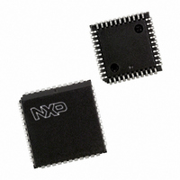
P89LV51RD2FA,512 NXP Semiconductors, P89LV51RD2FA,512 Datasheet - Page 43

P89LV51RD2FA,512
Manufacturer Part Number
P89LV51RD2FA,512
Description
IC 80C51 MCU 1024 RAM 44PLCC
Manufacturer
NXP Semiconductors
Series
89LVr
Datasheet
1.P89LV51RD2BBC557.pdf
(76 pages)
Specifications of P89LV51RD2FA,512
Core Processor
8051
Core Size
8-Bit
Speed
33MHz
Connectivity
SPI, UART/USART
Peripherals
Brown-out Detect/Reset, POR, PWM, WDT
Number Of I /o
32
Program Memory Size
64KB (64K x 8)
Program Memory Type
FLASH
Ram Size
1K x 8
Voltage - Supply (vcc/vdd)
2.7 V ~ 3.6 V
Oscillator Type
Internal
Operating Temperature
-40°C ~ 85°C
Package / Case
44-PLCC
Processor Series
P89LV5x
Core
80C51
Data Bus Width
8 bit
Data Ram Size
1 KB
Interface Type
SPI, UART
Maximum Clock Frequency
33 MHz
Number Of Programmable I/os
32
Number Of Timers
3
Operating Supply Voltage
2.4 V to 3.6 V
Maximum Operating Temperature
+ 85 C
Mounting Style
SMD/SMT
3rd Party Development Tools
PK51, CA51, A51, ULINK2
Minimum Operating Temperature
- 40 C
Package
44PLCC
Device Core
80C51
Family Name
89LV
Maximum Speed
40 MHz
For Use With
622-1017 - BOARD 44-ZIF PLCC SOCKET622-1008 - BOARD FOR LPC9103 10-HVSON
Lead Free Status / RoHS Status
Lead free / RoHS Compliant
Eeprom Size
-
Data Converters
-
Lead Free Status / Rohs Status
Details
Other names
935274176512
P89LV51RD2FA
P89LV51RD2FA
P89LV51RD2FA
P89LV51RD2FA
Available stocks
Company
Part Number
Manufacturer
Quantity
Price
Company:
Part Number:
P89LV51RD2FA,512
Manufacturer:
NXP Semiconductors
Quantity:
10 000
Part Number:
P89LV51RD2FA,512
Manufacturer:
NXP/恩智浦
Quantity:
20 000
NXP Semiconductors
P89LV51RB2_RC2_RD2_5
Product data sheet
Fig 16. SPI master-slave interconnection
CLOCK GENERATOR
SPI
and slave SPI devices. The SPICLK pin is the clock output and input for the master and
slave modes, respectively. The SPI clock generator will start following a write to the
master devices SPI data register. The written data is then shifted out of the MOSI pin on
the master device into the MOSI pin of the slave device. Following a complete
transmission of one byte of data, the SPI clock generator is stopped and the SPIF flag is
set. An SPI interrupt request will be generated if the SPI Interrupt Enable bit (SPIE) and
the Serial Port Interrupt Enable bit (ES) are both set.
An external master drives the Slave Select input pin, SS/P1[4], low to select the SPI
module as a slave. If SS/P1[4] has not been driven low, then the slave SPI unit is not
active and the MOSI/P1[5] port can also be used as an input port pin.
CPHA and CPOL control the phase and polarity of the SPI clock.
show the four possible combinations of these two bits.
Table 28.
Bit addressable; reset source(s): any reset; reset value: 0000 0000B.
Table 29.
Bit
7
6
5
4
3
Bit
Symbol
8-BIT SHIFT REGISTER
MSB master LSB
SPCTL - SPI control register (address D5H) bit allocation
SPCTL - SPI control register (address D5H) bit descriptions
Symbol
SPIE
SPEN
DORD
MSTR
CPOL
SPIE
7
Rev. 05 — 15 December 2009
SPEN
Description
If both SPIE and ES are set to one, SPI interrupts are enabled.
SPI enable bit. When set enables SPI.
Data transmission order. 0 = MSB first; 1 = LSB first in data
transmission.
Master/slave select. 1 = master mode, 0 = slave mode.
Clock polarity. 1 = SPICLK is high when idle (active LOW), 0 = SPICLK
is low when idle (active HIGH).
6
MISO
MOSI
SPICLK
SS
V
DD
DORD
5
SPICLK
V
P89LV51RB2/RC2/RD2
MISO
MOSI
SS
MSTR
SS
4
8-bit microcontrollers with 80C51 core
CPOL
3
8-BIT SHIFT REGISTER
MSB slave LSB
CPHA
2
Figure 17
© NXP B.V. 2009. All rights reserved.
PSC1
002aaa528
1
and
Figure 18
PSC0
43 of 76
0


