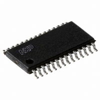
P89LPC931A1FDH,512 NXP Semiconductors, P89LPC931A1FDH,512 Datasheet - Page 27

P89LPC931A1FDH,512
Manufacturer Part Number
P89LPC931A1FDH,512
Description
IC 80C51 MCU FLASH 8K 28-TSSOP
Manufacturer
NXP Semiconductors
Series
LPC900r
Datasheet
1.P89LPC9301FDH512.pdf
(66 pages)
Specifications of P89LPC931A1FDH,512
Program Memory Type
FLASH
Program Memory Size
8KB (8K x 8)
Package / Case
28-TSSOP
Core Processor
8051
Core Size
8-Bit
Speed
18MHz
Connectivity
I²C, SPI, UART/USART
Peripherals
Brown-out Detect/Reset, POR, PWM, WDT
Number Of I /o
26
Ram Size
256 x 8
Voltage - Supply (vcc/vdd)
2.4 V ~ 3.6 V
Oscillator Type
Internal
Operating Temperature
-40°C ~ 85°C
Processor Series
P89LPC
Core
80C51
Data Bus Width
8 bit
Data Ram Size
256 B
Interface Type
I2C, SPI, UART
Maximum Clock Frequency
18 MHz
Number Of Programmable I/os
23
Number Of Timers
3
Operating Supply Voltage
2.4 V to 3.6 V
Maximum Operating Temperature
+ 85 C
Mounting Style
SMD/SMT
3rd Party Development Tools
PK51, CA51, A51, ULINK2
Minimum Operating Temperature
- 40 C
Lead Free Status / RoHS Status
Lead free / RoHS Compliant
For Use With
568-1758 - BOARD EVAL FOR LPC93X MCU FAMILY
Eeprom Size
-
Data Converters
-
Lead Free Status / Rohs Status
Lead free / RoHS Compliant
Other names
935288634512
NXP Semiconductors
P89LPC9301_931A1
Product data sheet
7.20.1 Mode 0
7.20.2 Mode 1
7.20.3 Mode 2
7.20.4 Mode 3
7.20.5 Mode 6
7.20.6 Timer overflow toggle output
7.20 Timers/counters 0 and 1
The boot address will be used if a UART break reset occurs, or the non-volatile boot
status bit (BOOTSTAT.0) = 1, or the device is forced into ISP mode during power-on (see
P89LPC9301/931A1 User manual). Otherwise, instructions will be fetched from address
0000H.
The P89LPC9301/931A1 has two general purpose counter/timers which are upward
compatible with the standard 80C51 Timer 0 and Timer 1. Both can be configured to
operate either as timers or event counters. An option to automatically toggle the T0 and/or
T1 pins upon timer overflow has been added.
In the ‘Timer’ function, the register is incremented every machine cycle.
In the ‘Counter’ function, the register is incremented in response to a 1-to-0 transition at its
corresponding external input pin, T0 or T1. In this function, the external input is sampled
once during every machine cycle.
Timer 0 and Timer 1 have five operating modes (Modes 0, 1, 2, 3 and 6). Modes 0, 1, 2
and 6 are the same for both Timers/Counters. Mode 3 is different.
Putting either Timer into Mode 0 makes it look like an 8048 Timer, which is an 8-bit
Counter with a divide-by-32 prescaler. In this mode, the Timer register is configured as a
13-bit register. Mode 0 operation is the same for Timer 0 and Timer 1.
Mode 1 is the same as Mode 0, except that all 16 bits of the timer register are used.
Mode 2 configures the Timer register as an 8-bit Counter with automatic reload. Mode 2
operation is the same for Timer 0 and Timer 1.
When Timer 1 is in Mode 3 it is stopped. Timer 0 in Mode 3 forms two separate 8-bit
counters and is provided for applications that require an extra 8-bit timer. When Timer 1 is
in Mode 3 it can still be used by the serial port as a baud rate generator.
In this mode, the corresponding timer can be changed to a PWM with a full period of
256 timer clocks.
Timers 0 and 1 can be configured to automatically toggle a port output whenever a timer
overflow occurs. The same device pins that are used for the T0 and T1 count inputs are
also used for the timer toggle outputs. The port outputs will be a logic 1 prior to the first
timer overflow when this mode is turned on.
All information provided in this document is subject to legal disclaimers.
Rev. 2 — 29 November 2010
8-bit microcontroller with accelerated two-clock 80C51 core
P89LPC9301/931A1
© NXP B.V. 2010. All rights reserved.
27 of 66


