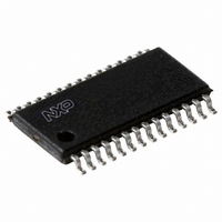
P89LPC931A1FDH,512 NXP Semiconductors, P89LPC931A1FDH,512 Datasheet - Page 26

P89LPC931A1FDH,512
Manufacturer Part Number
P89LPC931A1FDH,512
Description
IC 80C51 MCU FLASH 8K 28-TSSOP
Manufacturer
NXP Semiconductors
Series
LPC900r
Datasheet
1.P89LPC9301FDH512.pdf
(66 pages)
Specifications of P89LPC931A1FDH,512
Program Memory Type
FLASH
Program Memory Size
8KB (8K x 8)
Package / Case
28-TSSOP
Core Processor
8051
Core Size
8-Bit
Speed
18MHz
Connectivity
I²C, SPI, UART/USART
Peripherals
Brown-out Detect/Reset, POR, PWM, WDT
Number Of I /o
26
Ram Size
256 x 8
Voltage - Supply (vcc/vdd)
2.4 V ~ 3.6 V
Oscillator Type
Internal
Operating Temperature
-40°C ~ 85°C
Processor Series
P89LPC
Core
80C51
Data Bus Width
8 bit
Data Ram Size
256 B
Interface Type
I2C, SPI, UART
Maximum Clock Frequency
18 MHz
Number Of Programmable I/os
23
Number Of Timers
3
Operating Supply Voltage
2.4 V to 3.6 V
Maximum Operating Temperature
+ 85 C
Mounting Style
SMD/SMT
3rd Party Development Tools
PK51, CA51, A51, ULINK2
Minimum Operating Temperature
- 40 C
Lead Free Status / RoHS Status
Lead free / RoHS Compliant
For Use With
568-1758 - BOARD EVAL FOR LPC93X MCU FAMILY
Eeprom Size
-
Data Converters
-
Lead Free Status / Rohs Status
Lead free / RoHS Compliant
Other names
935288634512
NXP Semiconductors
P89LPC9301_931A1
Product data sheet
7.18.3 Total Power-down mode
7.19.1 Reset vector
7.19 Reset
This is the same as Power-down mode except that the brownout detection circuitry and
the voltage comparators are also disabled to conserve additional power. The internal RC
oscillator is disabled unless both the RC oscillator has been selected as the system clock
and the RTC is enabled. If the internal RC oscillator is used to clock the RTC during
power-down, there will be high power consumption. Please use an external low frequency
clock to achieve low power with the RTC running during power-down.
The P1.5/RST pin can function as either a LOW-active reset input or as a digital input,
P1.5. The Reset Pin Enable (RPE) bit in UCFG1, when set to logic 1, enables the external
reset input function on P1.5. When cleared, P1.5 may be used as an input pin.
Remark: During a power-up sequence, the RPE selection is overridden and this pin
always functions as a reset input. An external circuit connected to this pin should not
hold this pin LOW during a power-on sequence as this will keep the device in reset.
After power-up this pin will function as defined by the RPE bit. Only a power-up reset will
temporarily override the selection defined by RPE bit. Other sources of reset will not
override the RPE bit.
Note: During a power cycle, V
to ensure a power-on reset (see
Reset can be triggered from the following sources:
For every reset source, there is a flag in the Reset Register, RSTSRC. The user can read
this register to determine the most recent reset source. These flag bits can be cleared in
software by writing a logic 0 to the corresponding bit. More than one flag bit may be set:
Following reset, the P89LPC9301/931A1 will fetch instructions from either address 0000H
or the Boot address. The Boot address is formed by using the boot vector as the high byte
of the address and the low byte of the address = 00H.
•
•
•
•
•
•
•
•
•
External reset pin (during power-up or if user configured via UCFG1)
Power-on detect
Brownout detect
Watchdog timer
Software reset
UART break character detect reset
During a power-on reset, both POF and BOF are set but the other flag bits are
cleared.
A Watchdog reset is similar to a power-on reset, both POF and BOF are set but the
other flag bits are cleared.
For any other reset, previously set flag bits that have not been cleared will remain set.
All information provided in this document is subject to legal disclaimers.
Rev. 2 — 29 November 2010
8-bit microcontroller with accelerated two-clock 80C51 core
DD
Table 10 “Static
must fall below V
P89LPC9301/931A1
characteristics”).
POR
before power is reapplied, in order
© NXP B.V. 2010. All rights reserved.
26 of 66


