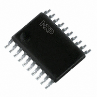
P89LPC9241FDH,112 NXP Semiconductors, P89LPC9241FDH,112 Datasheet - Page 39

P89LPC9241FDH,112
Manufacturer Part Number
P89LPC9241FDH,112
Description
IC 80C51 MCU FLASH 4K 20-TSSOP
Manufacturer
NXP Semiconductors
Series
LPC900r
Datasheet
1.P89LPC9201FDH112.pdf
(75 pages)
Specifications of P89LPC9241FDH,112
Program Memory Type
FLASH
Program Memory Size
4KB (4K x 8)
Package / Case
20-TSSOP
Core Processor
8051
Core Size
8-Bit
Speed
18MHz
Connectivity
I²C, UART/USART
Peripherals
Brown-out Detect/Reset, POR, PWM, WDT
Number Of I /o
18
Ram Size
256 x 8
Voltage - Supply (vcc/vdd)
2.4 V ~ 3.6 V
Data Converters
A/D 4x8b; D/A 1x8b
Oscillator Type
Internal
Operating Temperature
-40°C ~ 85°C
Processor Series
P89LPC
Core
80C51
Data Bus Width
8 bit
Data Ram Size
256 B
Interface Type
I2C, SPI, UART
Maximum Clock Frequency
18 MHz
Number Of Programmable I/os
15
Number Of Timers
2
Operating Supply Voltage
2.4 V to 3.6 V
Maximum Operating Temperature
+ 85 C
Mounting Style
SMD/SMT
3rd Party Development Tools
PK51, CA51, A51, ULINK2
Minimum Operating Temperature
- 40 C
On-chip Adc
8 bit, 4 Channel
Lead Free Status / RoHS Status
Lead free / RoHS Compliant
Eeprom Size
-
Lead Free Status / Rohs Status
Lead free / RoHS Compliant
Other names
935288642112
NXP Semiconductors
P89LPC92X1
Product data sheet
7.22.10 The 9
7.22.9 Transmit interrupts with double buffering enabled (modes 1, 2 and 3)
7.23 I
Unlike the conventional UART, in double buffering mode, the TI interrupt is generated
when the double buffer is ready to receive new data.
If double buffering is disabled TB8 can be written before or after SBUF is written, as long
as TB8 is updated some time before that bit is shifted out. TB8 must not be changed until
the bit is shifted out, as indicated by the TI interrupt.
If double buffering is enabled, TB8 must be updated before SBUF is written, as TB8 will
be double-buffered together with SBUF data.
The I
connected to the bus, and it has the following features:
A typical I
P89LPC9201/9211/922A1/9241/9251 device provides a byte-oriented I
that supports data transfers up to 400 kHz.
2
Fig 11. I
•
•
•
•
•
•
C-bus serial interface
Bidirectional data transfer between masters and slaves
Multi master bus (no central master)
Arbitration between simultaneously transmitting masters without corruption of serial
data on the bus
Serial clock synchronization allows devices with different bit rates to communicate via
one serial bus
Serial clock synchronization can be used as a handshake mechanism to suspend and
resume serial transfer
The I
2
C-bus uses two wires (SDA and SCL) to transfer information between devices
th
bit (bit 8) in double buffering (modes 1, 2 and 3)
2
2
2
C-bus may be used for test and diagnostic purposes.
C-bus configuration is shown in
C-bus configuration
I
2
C-bus
All information provided in this document is subject to legal disclaimers.
P1.3/SDA
P89LPC9201/9211/
Rev. 2 — 1 December 2010
922A1/9241/9251
P89LPC9201/9211/922A1/9241/
P1.2/SCL
OTHER DEVICE
WITH I
R P
Figure
INTERFACE
2
C-BUS
11. The
R P
8-bit microcontroller with 8-bit ADC
OTHER DEVICE
WITH I
INTERFACE
2
C-BUS
002aae430
2
© NXP B.V. 2010. All rights reserved.
C-bus interface
SDA
SCL
39 of 75


