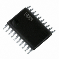
P89LPC9241FDH,112 NXP Semiconductors, P89LPC9241FDH,112 Datasheet - Page 48

P89LPC9241FDH,112
Manufacturer Part Number
P89LPC9241FDH,112
Description
IC 80C51 MCU FLASH 4K 20-TSSOP
Manufacturer
NXP Semiconductors
Series
LPC900r
Datasheet
1.P89LPC9201FDH112.pdf
(75 pages)
Specifications of P89LPC9241FDH,112
Program Memory Type
FLASH
Program Memory Size
4KB (4K x 8)
Package / Case
20-TSSOP
Core Processor
8051
Core Size
8-Bit
Speed
18MHz
Connectivity
I²C, UART/USART
Peripherals
Brown-out Detect/Reset, POR, PWM, WDT
Number Of I /o
18
Ram Size
256 x 8
Voltage - Supply (vcc/vdd)
2.4 V ~ 3.6 V
Data Converters
A/D 4x8b; D/A 1x8b
Oscillator Type
Internal
Operating Temperature
-40°C ~ 85°C
Processor Series
P89LPC
Core
80C51
Data Bus Width
8 bit
Data Ram Size
256 B
Interface Type
I2C, SPI, UART
Maximum Clock Frequency
18 MHz
Number Of Programmable I/os
15
Number Of Timers
2
Operating Supply Voltage
2.4 V to 3.6 V
Maximum Operating Temperature
+ 85 C
Mounting Style
SMD/SMT
3rd Party Development Tools
PK51, CA51, A51, ULINK2
Minimum Operating Temperature
- 40 C
On-chip Adc
8 bit, 4 Channel
Lead Free Status / RoHS Status
Lead free / RoHS Compliant
Eeprom Size
-
Lead Free Status / Rohs Status
Lead free / RoHS Compliant
Other names
935288642112
NXP Semiconductors
P89LPC92X1
Product data sheet
Fig 15. ADC block diagram
V
ref(bg)
V
sen
8.5.1 Fixed channel, single conversion mode
8.5.2 Fixed channel, continuous conversion mode
8.3 Block diagram
8.4 Temperature sensor
8.5 ADC operating modes
2:1 MUX
AD10
AD11
AD12
AD13
An on-chip wide-temperature range temperature sensor is integrated. It provides
temperature sensing capability of −40 °C ~ 85 °C. ADC0 is dedicated for the temperature
sensor, and the temperature sensor is measured through Anin03. To get an accurate
temperature value, it is necessary to get supply voltage by measuring the internal
reference voltage V
manual for detailed usage of temperature sensor.
A single input channel can be selected for conversion. A single conversion will be
performed and the result placed in the result register which corresponds to the selected
input channel. An interrupt, if enabled, will be generated after the conversion completes.
A single input channel can be selected for continuous conversion. The results of the
conversions will be sequentially placed in the four result register. The user may select
whether an interrupt can be generated after every four conversions. Additional conversion
results will again cycle through the four result register, overwriting the previous results.
Continuous conversions continue until terminated by the user.
Anin00
Anin01
Anin02
Anin03
Anin10
Anin11
Anin12
Anin13
input MUX
input MUX
All information provided in this document is subject to legal disclaimers.
ref(bg)
Rev. 2 — 1 December 2010
P89LPC9201/9211/922A1/9241/
first. Please see the P89LPC9201/9211/922A1/9241/9251 User
comp
comp
+
–
+
–
DAC0
DAC1
8-bit microcontroller with 8-bit ADC
CCLK
SAR
SAR
8
8
CONTROL
© NXP B.V. 2010. All rights reserved.
LOGIC
002aae432
48 of 75


