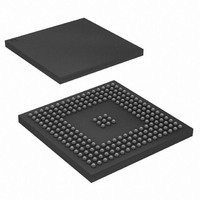
AT91SAM9XE512-CU Atmel, AT91SAM9XE512-CU Datasheet - Page 262

AT91SAM9XE512-CU
Manufacturer Part Number
AT91SAM9XE512-CU
Description
MCU ARM9 512K FLASH 217-BGA
Manufacturer
Atmel
Series
AT91SAMr
Datasheet
1.AT91SAM9XE128-QU.pdf
(860 pages)
Specifications of AT91SAM9XE512-CU
Core Processor
ARM9
Core Size
16/32-Bit
Speed
180MHz
Connectivity
EBI/EMI, Ethernet, I²C, MMC, SPI, SSC, UART/USART, USB
Peripherals
Brown-out Detect/Reset, POR, PWM, WDT
Number Of I /o
96
Program Memory Size
512KB (512K x 8)
Program Memory Type
FLASH
Ram Size
56K x 8
Voltage - Supply (vcc/vdd)
1.65 V ~ 1.95 V
Data Converters
A/D 4x10b
Oscillator Type
Internal
Operating Temperature
-40°C ~ 85°C
Package / Case
217-LFBGA
Package
217LFBGA
Device Core
ARM926EJ-S
Family Name
91S
Maximum Speed
180 MHz
Operating Supply Voltage
1.8|2.5|3.3 V
Data Bus Width
32 Bit
Number Of Programmable I/os
96
Interface Type
EBI/Ethernet/SPI/TWI/USART/USB
On-chip Adc
4-chx10-bit
Number Of Timers
6
Processor Series
AT91SAMx
Core
ARM926EJ-S
Data Ram Size
32 KB
Maximum Clock Frequency
180 MHz
Maximum Operating Temperature
+ 85 C
Mounting Style
SMD/SMT
3rd Party Development Tools
JTRACE-ARM-2M, KSK-AT91SAM9XE-PL, MDK-ARM, RL-ARM, ULINK2
Development Tools By Supplier
AT91SAM-ICE, AT91-ISP, AT91SAM9XE-EK
Minimum Operating Temperature
- 40 C
For Use With
AT91SAM9XE-EK - KIT EVAL FOR AT91SAM9XEAT91SAM-ICE - EMULATOR FOR AT91 ARM7/ARM9
Lead Free Status / RoHS Status
Lead free / RoHS Compliant
Eeprom Size
-
Lead Free Status / Rohs Status
Details
Available stocks
Company
Part Number
Manufacturer
Quantity
Price
Company:
Part Number:
AT91SAM9XE512-CU
Manufacturer:
NEC
Quantity:
201
Part Number:
AT91SAM9XE512-CU
Manufacturer:
ATMEL/爱特梅尔
Quantity:
20 000
- Current page: 262 of 860
- Download datasheet (13Mb)
25.3.1
25.3.2
6254C–ATARM–22-Jan-10
Write Access
Read Access
mend to utilize either 1 ECC per 256 bytes of data, 1 ECC per 512 bytes of data or 1 ECC for all
of the page.
The only configurations required for ECC are the NAND Flash or the SmartMedia page size
(528/2112/4224) and the type of correction wanted (1 ECC for all the page/1 ECC per 256 bytes
of data /1 ECC per 512 bytes of data). Page size is configured setting the PAGESIZE field in the
ECC Mode Register (ECC_MR). Type of correction is configured setting the TYPCORRECT
field in the ECC Mode Register (ECC_MR).
ECC is automatically computed as soon as a read (00h)/write (80h) command to the NAND
Flash or the SmartMedia is detected. Read and write access must start at a page boundary.
ECC results are available as soon as the counter reaches the end of the main area. Values in
the ECC Parity Registers (ECC_PR0 to ECC_PR15) are then valid and locked until a new start
condition occurs (read/write command followed by address cycles).
Once the Flash memory page is written, the computed ECC codes are available in the ECC Par-
ity (ECC_PR0 to ECC_PR15) registers. The ECC code values must be written by the software
application in the extra area used for redundancy. The number of write accesses in the extra
area is a function of the value of the type of correction field. For example, for 1 ECC per 256
bytes of data for a page of 512 bytes, only the values of ECC_PR0 and ECC_PR1 must be writ-
ten by the software application. Other registers are meaningless.
After reading the whole data in the main area, the application must perform read accesses to the
extra area where ECC code has been previously stored. Error detection is automatically per-
formed by the ECC controller. Please note that it is mandatory to read consecutively the entire
main area and the locations where Parity and NParity values have been previously stored to let
the ECC controller perform error detection.
The application can check the ECC Status Registers (ECC_SR1/ECC_SR2) for any detected
errors. It is up to the application to correct any detected error. ECC computation can detect four
different circumstances:
• No error: XOR between the ECC computation and the ECC code stored at the end of the
• Recoverable error: Only the RECERR flags in the ECC Status registers
• ECC error: The ECCERR flag in the ECC Status Registers (ECC_SR1/ECC_SR2) are set.
• Non correctable error: The MULERR flag in the ECC Status Registers
NAND Flash or SmartMedia page is equal to 0. No error flags in the ECC Status Registers
(ECC_SR1/ECC_SR2).
(ECC_SR1/ECC_SR2) are set. The corrupted word offset in the read page is defined by the
WORDADDR field in the ECC Parity Registers (ECC_PR0 to ECC_PR15). The corrupted bit
position in the concerned word is defined in the BITADDR field in the ECC Parity Registers
(ECC_PR0 to ECC_PR15).
An error has been detected in the ECC code stored in the Flash memory. The position of the
corrupted bit can be found by the application performing an XOR between the Parity and the
NParity contained in the ECC code stored in the Flash memory.
(ECC_SR1/ECC_SR2) are set. Several unrecoverable errors have been detected in the
Flash memory page.
AT91SAM9XE128/256/512 Preliminary
262
Related parts for AT91SAM9XE512-CU
Image
Part Number
Description
Manufacturer
Datasheet
Request
R

Part Number:
Description:
KIT EVAL FOR AT91SAM9XE
Manufacturer:
Atmel
Datasheet:

Part Number:
Description:
MCU ARM9 64K SRAM 144-LFBGA
Manufacturer:
Atmel
Datasheet:

Part Number:
Description:
IC ARM7 MCU FLASH 256K 100LQFP
Manufacturer:
Atmel
Datasheet:

Part Number:
Description:
IC ARM9 MPU 217-LFBGA
Manufacturer:
Atmel
Datasheet:

Part Number:
Description:
MCU ARM9 ULTRA LOW PWR 217-LFBGA
Manufacturer:
Atmel
Datasheet:

Part Number:
Description:
MCU ARM9 324-TFBGA
Manufacturer:
Atmel
Datasheet:

Part Number:
Description:
IC MCU ARM9 SAMPLING 217CBGA
Manufacturer:
Atmel
Datasheet:

Part Number:
Description:
IC ARM9 MCU 217-LFBGA
Manufacturer:
Atmel
Datasheet:

Part Number:
Description:
IC ARM9 MCU 208-PQFP
Manufacturer:
Atmel
Datasheet:

Part Number:
Description:
MCU ARM 512K HS FLASH 100-LQFP
Manufacturer:
Atmel
Datasheet:

Part Number:
Description:
MCU ARM 512K HS FLASH 100-TFBGA
Manufacturer:
Atmel
Datasheet:

Part Number:
Description:
IC ARM9 MCU 200 MHZ 324-TFBGA
Manufacturer:
Atmel
Datasheet:

Part Number:
Description:
IC ARM MCU 16BIT 128K 256BGA
Manufacturer:
Atmel
Datasheet:

Part Number:
Description:
IC ARM7 MCU 32BIT 128K 64LQFP
Manufacturer:
Atmel
Datasheet:

Part Number:
Description:
IC ARM7 MCU FLASH 256K 128-LQFP
Manufacturer:
Atmel
Datasheet:


