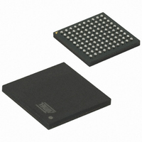
AT91SAM7X512-CU Atmel, AT91SAM7X512-CU Datasheet - Page 236

AT91SAM7X512-CU
Manufacturer Part Number
AT91SAM7X512-CU
Description
MCU ARM 512K HS FLASH 100-TFBGA
Manufacturer
Atmel
Series
AT91SAMr
Datasheet
1.AT91SAM7X512-AU-999.pdf
(687 pages)
Specifications of AT91SAM7X512-CU
Core Processor
ARM7
Core Size
16/32-Bit
Speed
55MHz
Connectivity
CAN, Ethernet, I²C, SPI, SSC, UART/USART, USB
Peripherals
Brown-out Detect/Reset, DMA, POR, PWM, WDT
Number Of I /o
62
Program Memory Size
512KB (512K x 8)
Program Memory Type
FLASH
Ram Size
128K x 8
Voltage - Supply (vcc/vdd)
1.65 V ~ 1.95 V
Data Converters
A/D 8x10b
Oscillator Type
Internal
Operating Temperature
-40°C ~ 85°C
Package / Case
100-TFBGA
Processor Series
AT91SAMx
Core
ARM7TDMI
Data Bus Width
32 bit
Data Ram Size
128 KB
Interface Type
CAN, SPI, SSC, TWI, USART, USB
Maximum Clock Frequency
55 MHz
Number Of Programmable I/os
13
Number Of Timers
3
Operating Supply Voltage
3 V to 3.6 V
Maximum Operating Temperature
+ 85 C
Mounting Style
SMD/SMT
3rd Party Development Tools
JTRACE-ARM-2M, KSK-AT91SAM7X-PL, MDK-ARM, RL-ARM, ULINK2
Development Tools By Supplier
AT91SAM-ICE, AT91-ISP, AT91SAM7X-EK
Minimum Operating Temperature
- 40 C
On-chip Adc
10 bit
Package
100TFBGA
Device Core
ARM7TDMI
Family Name
91S
Maximum Speed
55 MHz
Cpu Family
91S
Device Core Size
32b
Frequency (max)
55MHz
Total Internal Ram Size
128KB
# I/os (max)
62
Number Of Timers - General Purpose
3
Operating Supply Voltage (typ)
1.8/3.3V
Operating Supply Voltage (max)
1.95/3.6V
Operating Supply Voltage (min)
1.65/3V
Instruction Set Architecture
RISC
Operating Temp Range
-40C to 85C
Operating Temperature Classification
Industrial
Mounting
Surface Mount
Pin Count
100
Package Type
TFBGA
For Use With
AT91SAM-ICE - EMULATOR FOR AT91 ARM7/ARM9AT91SAM7X-EK - KIT EVAL FOR AT91SAM7X256/128
Lead Free Status / RoHS Status
Lead free / RoHS Compliant
Eeprom Size
-
Lead Free Status / Rohs Status
Lead free / RoHS Compliant
Available stocks
Company
Part Number
Manufacturer
Quantity
Price
- Current page: 236 of 687
- Download datasheet (11Mb)
Figure 27-5. Input Glitch Filter Timing
27.4.10
Figure 27-6. Input Change Interrupt Timings
236
if PIO_IFSR = 0
if PIO_IFSR = 1
Read PIO_ISR
PIO_PDSR
PIO_PDSR
Pin Level
Pin Level
PIO_ISR
AT91SAM7X512/256/128 Preliminary
MCK
Input Change Interrupt
MCK
The PIO Controller can be programmed to generate an interrupt when it detects an input change
on an I/O line. The Input Change Interrupt is controlled by writing PIO_IER (Interrupt Enable
Register) and PIO_IDR (Interrupt Disable Register), which respectively enable and disable the
input change interrupt by setting and clearing the corresponding bit in PIO_IMR (Interrupt Mask
Register). As Input change detection is possible only by comparing two successive samplings of
the input of the I/O line, the PIO Controller clock must be enabled. The Input Change Interrupt is
available, regardless of the configuration of the I/O line, i.e. configured as an input only, con-
trolled by the PIO Controller or assigned to a peripheral function.
When an input change is detected on an I/O line, the corresponding bit in PIO_ISR (Interrupt
Status Register) is set. If the corresponding bit in PIO_IMR is set, the PIO Controller interrupt
line is asserted. The interrupt signals of the thirty-two channels are ORed-wired together to gen-
erate a single interrupt signal to the Advanced Interrupt Controller.
When the software reads PIO_ISR, all the interrupts are automatically cleared. This signifies that
all the interrupts that are pending when PIO_ISR is read must be handled.
1 cycle
1 cycle
APB Access
up to 1.5 cycles
1 cycle
up to 2.5 cycles
2 cycles
APB Access
6120H–ATARM–17-Feb-09
up to 2 cycles
1 cycle
1 cycle
Related parts for AT91SAM7X512-CU
Image
Part Number
Description
Manufacturer
Datasheet
Request
R

Part Number:
Description:
KIT EVAL FOR AT91SAM7X256/128
Manufacturer:
Atmel
Datasheet:

Part Number:
Description:
MCU, MPU & DSP Development Tools KICKSTART KIT ATMEL AT91SAM7X
Manufacturer:
IAR Systems

Part Number:
Description:
DEV KIT FOR AVR/AVR32
Manufacturer:
Atmel
Datasheet:

Part Number:
Description:
INTERVAL AND WIPE/WASH WIPER CONTROL IC WITH DELAY
Manufacturer:
ATMEL Corporation
Datasheet:

Part Number:
Description:
Low-Voltage Voice-Switched IC for Hands-Free Operation
Manufacturer:
ATMEL Corporation
Datasheet:

Part Number:
Description:
MONOLITHIC INTEGRATED FEATUREPHONE CIRCUIT
Manufacturer:
ATMEL Corporation
Datasheet:

Part Number:
Description:
AM-FM Receiver IC U4255BM-M
Manufacturer:
ATMEL Corporation
Datasheet:

Part Number:
Description:
Monolithic Integrated Feature Phone Circuit
Manufacturer:
ATMEL Corporation
Datasheet:

Part Number:
Description:
Multistandard Video-IF and Quasi Parallel Sound Processing
Manufacturer:
ATMEL Corporation
Datasheet:

Part Number:
Description:
High-performance EE PLD
Manufacturer:
ATMEL Corporation
Datasheet:

Part Number:
Description:
8-bit Flash Microcontroller
Manufacturer:
ATMEL Corporation
Datasheet:

Part Number:
Description:
2-Wire Serial EEPROM
Manufacturer:
ATMEL Corporation
Datasheet:


