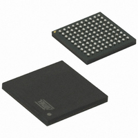
AT91SAM7X512-CU Atmel, AT91SAM7X512-CU Datasheet - Page 130

AT91SAM7X512-CU
Manufacturer Part Number
AT91SAM7X512-CU
Description
MCU ARM 512K HS FLASH 100-TFBGA
Manufacturer
Atmel
Series
AT91SAMr
Datasheet
1.AT91SAM7X512-AU-999.pdf
(687 pages)
Specifications of AT91SAM7X512-CU
Core Processor
ARM7
Core Size
16/32-Bit
Speed
55MHz
Connectivity
CAN, Ethernet, I²C, SPI, SSC, UART/USART, USB
Peripherals
Brown-out Detect/Reset, DMA, POR, PWM, WDT
Number Of I /o
62
Program Memory Size
512KB (512K x 8)
Program Memory Type
FLASH
Ram Size
128K x 8
Voltage - Supply (vcc/vdd)
1.65 V ~ 1.95 V
Data Converters
A/D 8x10b
Oscillator Type
Internal
Operating Temperature
-40°C ~ 85°C
Package / Case
100-TFBGA
Processor Series
AT91SAMx
Core
ARM7TDMI
Data Bus Width
32 bit
Data Ram Size
128 KB
Interface Type
CAN, SPI, SSC, TWI, USART, USB
Maximum Clock Frequency
55 MHz
Number Of Programmable I/os
13
Number Of Timers
3
Operating Supply Voltage
3 V to 3.6 V
Maximum Operating Temperature
+ 85 C
Mounting Style
SMD/SMT
3rd Party Development Tools
JTRACE-ARM-2M, KSK-AT91SAM7X-PL, MDK-ARM, RL-ARM, ULINK2
Development Tools By Supplier
AT91SAM-ICE, AT91-ISP, AT91SAM7X-EK
Minimum Operating Temperature
- 40 C
On-chip Adc
10 bit
Package
100TFBGA
Device Core
ARM7TDMI
Family Name
91S
Maximum Speed
55 MHz
Cpu Family
91S
Device Core Size
32b
Frequency (max)
55MHz
Total Internal Ram Size
128KB
# I/os (max)
62
Number Of Timers - General Purpose
3
Operating Supply Voltage (typ)
1.8/3.3V
Operating Supply Voltage (max)
1.95/3.6V
Operating Supply Voltage (min)
1.65/3V
Instruction Set Architecture
RISC
Operating Temp Range
-40C to 85C
Operating Temperature Classification
Industrial
Mounting
Surface Mount
Pin Count
100
Package Type
TFBGA
For Use With
AT91SAM-ICE - EMULATOR FOR AT91 ARM7/ARM9AT91SAM7X-EK - KIT EVAL FOR AT91SAM7X256/128
Lead Free Status / RoHS Status
Lead free / RoHS Compliant
Eeprom Size
-
Lead Free Status / Rohs Status
Lead free / RoHS Compliant
Available stocks
Company
Part Number
Manufacturer
Quantity
Price
- Current page: 130 of 687
- Download datasheet (11Mb)
20.3.4
20.3.4.1
130
AT91SAM7X512/256/128 Preliminary
Device Operations
Flash Read Command
Access to these registers is done through the TAP 38-bit DR register comprising a 32-bit data
field, a 5-bit address field and a read/write bit. The data to be written is scanned into the 32-bit
data field with the address of the register to the 5-bit address field and 1 to the read/write bit. A
register is read by scanning its address into the address field and 0 into the read/write bit, going
through the UPDATE-DR TAP state, then scanning out the data.
Refer to the ARM7TDMI reference manuel for more information on Comm channel operations.
Figure 20-5. TAP 8-bit DR Register
A read or write takes place when the TAP controller enters UPDATE-DR state. Refer to the IEEE
1149.1 for more details on JTAG operations.
The write handshake is done by polling the Debug Comms Control Register until the R bit is
cleared. Once cleared, data can be written to the Debug Comms Data Register.
The read handshake is done by polling the Debug Comms Control Register until the W bit is set.
Once set, data can be read in the Debug Comms Data Register.
Several commands on the Flash memory are available. These commands are summarized in
Table 20-3 on page
is reading and writing the Debug Comms Registers.
This command is used to read the Flash contents. The memory map is accessible through this
command. Memory is seen as an array of words (32-bit wide). The read command can start at
• Debug Comms Control Register: DCCR
• Debug Comms Data Register: DCDR
• The address of the Debug Comms Control Register is 0x04.
• The address of the Debug Comms Data Register is 0x05.
TDI
The Debug Comms Control Register is read-only and allows synchronized handshaking
between the processor and the debugger.
– Bit 1 (W): Denotes whether the programmer can read a data through the Debug
– Bit 0 (R): Denotes whether the programmer can send data from the Debug Comms
Comms Data Register. If the device is busy W = 0, then the programmer must poll
until W = 1.
Data Register. If R = 1, data previously placed there through the scan chain has not
been collected by the device and so the programmer must wait.
r/w
4
Address
Address
Decoder
121. Commands are run by the programmer through the serial interface that
5
0
31
Debug Comms Control Register
Debug Comms Data Register
Data
32
6120H–ATARM–17-Feb-09
0
TDO
Related parts for AT91SAM7X512-CU
Image
Part Number
Description
Manufacturer
Datasheet
Request
R

Part Number:
Description:
KIT EVAL FOR AT91SAM7X256/128
Manufacturer:
Atmel
Datasheet:

Part Number:
Description:
MCU, MPU & DSP Development Tools KICKSTART KIT ATMEL AT91SAM7X
Manufacturer:
IAR Systems

Part Number:
Description:
DEV KIT FOR AVR/AVR32
Manufacturer:
Atmel
Datasheet:

Part Number:
Description:
INTERVAL AND WIPE/WASH WIPER CONTROL IC WITH DELAY
Manufacturer:
ATMEL Corporation
Datasheet:

Part Number:
Description:
Low-Voltage Voice-Switched IC for Hands-Free Operation
Manufacturer:
ATMEL Corporation
Datasheet:

Part Number:
Description:
MONOLITHIC INTEGRATED FEATUREPHONE CIRCUIT
Manufacturer:
ATMEL Corporation
Datasheet:

Part Number:
Description:
AM-FM Receiver IC U4255BM-M
Manufacturer:
ATMEL Corporation
Datasheet:

Part Number:
Description:
Monolithic Integrated Feature Phone Circuit
Manufacturer:
ATMEL Corporation
Datasheet:

Part Number:
Description:
Multistandard Video-IF and Quasi Parallel Sound Processing
Manufacturer:
ATMEL Corporation
Datasheet:

Part Number:
Description:
High-performance EE PLD
Manufacturer:
ATMEL Corporation
Datasheet:

Part Number:
Description:
8-bit Flash Microcontroller
Manufacturer:
ATMEL Corporation
Datasheet:

Part Number:
Description:
2-Wire Serial EEPROM
Manufacturer:
ATMEL Corporation
Datasheet:


