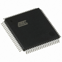
AT89C5132-RORUL Atmel, AT89C5132-RORUL Datasheet - Page 13

AT89C5132-RORUL
Manufacturer Part Number
AT89C5132-RORUL
Description
MCU 8051 FLASH USB 80TQFP
Manufacturer
Atmel
Series
AT89C513xr
Specifications of AT89C5132-RORUL
Core Processor
C52X2
Core Size
8-Bit
Speed
20MHz
Connectivity
IDE/ATAPI, I²C, MMC, PCM, SPI, UART/USART, USB
Peripherals
I²S, POR, WDT
Number Of I /o
44
Program Memory Size
64KB (64K x 8)
Program Memory Type
FLASH
Eeprom Size
4K x 8
Ram Size
2.25K x 8
Voltage - Supply (vcc/vdd)
2.7 V ~ 3.3 V
Data Converters
A/D 2x10b
Oscillator Type
Internal
Operating Temperature
-40°C ~ 85°C
Package / Case
80-TQFP, 80-VQFP
Lead Free Status / RoHS Status
Lead free / RoHS Compliant
Available stocks
Company
Part Number
Manufacturer
Quantity
Price
- Current page: 13 of 182
- Download datasheet (2Mb)
6.3
6.3.1
4173E–USB–09/07
PLL
PLL Description
eral clock frequency is the oscillator frequency divided by 2 while in X2 mode, it is the oscillator
frequency.
Note:
Figure 6-3.
Note:
The AT89C5132 PLL is used to generate internal high frequency clock (the PLL Clock) synchro-
nized with an external low-frequency (the Oscillator Clock). The PLL clock provides the audio
interface, and the USB interface clocks. Figure 6-4 shows the internal structure of the PLL.
The PFLD block is the Phase Frequency Comparator and Lock Detector. This block makes the
comparison between the reference clock coming from the N divider and the reverse clock com-
ing from the R divider and generates some pulses on the Up or Down signal depending on the
edge position of the reverse clock. The PLLEN bit in PLLCON register is used to enable the
clock generation. When the PLL is locked, the bit PLOCK in PLLCON register (see Table 3) is
set.
The CHP block is the Charge Pump that generates the voltage reference for the VCO by inject-
ing or extracting charges from the external filter connected on PFILT pin (see Figure 6-5). Value
of the filter components are detailed in the Section “DC Characteristics”.
The VCO block is the Voltage Controlled Oscillator controlled by the voltage V
charge pump. It generates a square wave signal: the PLL clock.
1. The X2 bit reset value depends on the X2B bit in the Hardware Security Byte (see Table 12 on
In order to prevent any incorrect operation while operating in X2 mode, the user must be aware
that all peripherals using clock frequency as time reference (timers…) will have their time refer-
ence divided by two. For example, a free running timer generating an interrupt every 20 ms will
then generate an interrupt every 10 ms.
X1 ÷ 2
X2 Bit
Clock
page 24). Using the AT89C5132 (Flash Version) the system can boot either in standard or X2
mode depending on the X2B value. Using AT83C51SND1C (ROM Version) the system always
boots in standard mode. X2B bit can be changed to X2 mode later by software.
X1
Mode Switching Waveforms
STD Mode
X2 Mode
(1)
AT89C5132
ref
produced by the
STD Mode
13
Related parts for AT89C5132-RORUL
Image
Part Number
Description
Manufacturer
Datasheet
Request
R

Part Number:
Description:
Manufacturer:
Atmel Corporation
Datasheet:

Part Number:
Description:
IC 8051 MCU FLASH 64K USB 80TQFP
Manufacturer:
Atmel
Datasheet:

Part Number:
Description:
DEV KIT FOR AVR/AVR32
Manufacturer:
Atmel
Datasheet:

Part Number:
Description:
INTERVAL AND WIPE/WASH WIPER CONTROL IC WITH DELAY
Manufacturer:
ATMEL Corporation
Datasheet:

Part Number:
Description:
Low-Voltage Voice-Switched IC for Hands-Free Operation
Manufacturer:
ATMEL Corporation
Datasheet:

Part Number:
Description:
MONOLITHIC INTEGRATED FEATUREPHONE CIRCUIT
Manufacturer:
ATMEL Corporation
Datasheet:

Part Number:
Description:
AM-FM Receiver IC U4255BM-M
Manufacturer:
ATMEL Corporation
Datasheet:

Part Number:
Description:
Monolithic Integrated Feature Phone Circuit
Manufacturer:
ATMEL Corporation
Datasheet:

Part Number:
Description:
Multistandard Video-IF and Quasi Parallel Sound Processing
Manufacturer:
ATMEL Corporation
Datasheet:

Part Number:
Description:
High-performance EE PLD
Manufacturer:
ATMEL Corporation
Datasheet:

Part Number:
Description:
8-bit Flash Microcontroller
Manufacturer:
ATMEL Corporation
Datasheet:


