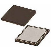
PIC24FJ256GB206-I/MR Microchip Technology, PIC24FJ256GB206-I/MR Datasheet - Page 333

PIC24FJ256GB206-I/MR
Manufacturer Part Number
PIC24FJ256GB206-I/MR
Description
MCU PIC 16BIT FLASH 256K 64VQFN
Manufacturer
Microchip Technology
Series
PIC® 24Fr
Specifications of PIC24FJ256GB206-I/MR
Core Size
16-Bit
Program Memory Size
256KB (85.5K x 24)
Core Processor
PIC
Speed
32MHz
Connectivity
I²C, IrDA, SPI, UART/USART, USB OTG
Peripherals
Brown-out Detect/Reset, LVD, POR, PWM, WDT
Number Of I /o
52
Program Memory Type
FLASH
Ram Size
96K x 8
Voltage - Supply (vcc/vdd)
2.2 V ~ 3.6 V
Data Converters
A/D 16x10b
Oscillator Type
Internal
Operating Temperature
-40°C ~ 85°C
Package / Case
64-VFQFN, Exposed Pad
Controller Family/series
PIC24
No. Of I/o's
52
Ram Memory Size
96KB
Cpu Speed
32MHz
No. Of Timers
5
No. Of Pwm Channels
9
Processor Series
PIC24FJ
Core
PIC
Data Bus Width
16 bit
Data Ram Size
96 KB
Interface Type
I2C, SPI, UART
Maximum Clock Frequency
32 MHz
Number Of Programmable I/os
29
Number Of Timers
5
Operating Supply Voltage
2.2 V to 3.6 V
Maximum Operating Temperature
+ 85 C
Mounting Style
SMD/SMT
3rd Party Development Tools
52713-733, 52714-737, 53276-922, EWDSPIC
Development Tools By Supplier
PG164130, DV164035, DV244005, DV164005, DM240001, MA240021
Minimum Operating Temperature
- 40 C
On-chip Adc
10 bit, 16 Channel
Lead Free Status / RoHS Status
Lead free / RoHS Compliant
Eeprom Size
-
Lead Free Status / Rohs Status
Details
- Current page: 333 of 386
- Download datasheet (4Mb)
26.4.3
The Configuration registers are protected against
inadvertent or unwanted changes or reads in two ways.
The primary protection method is the same as that of
the RP registers – shadow registers contain a compli-
mentary value which is constantly compared with the
actual value.
TABLE 26-2:
26.5
PIC24FJ256GB210 family devices implement a JTAG
interface, which supports boundary scan device
testing.
26.6
PIC24FJ256GB210 family microcontrollers can be
serially programmed while in the end application circuit.
This is simply done with two lines for clock (PGECx)
and data (PGEDx), and three other lines for power
(V
to manufacture boards with unprogrammed devices
and then program the microcontroller just before
shipping the product. This also allows the most recent
firmware or a custom firmware to be programmed.
2010 Microchip Technology Inc.
DD
WPDIS
Segment Configuration Bits
), ground (V
1
0
0
0
JTAG Interface
In-Circuit Serial Programming™
CONFIGURATION REGISTER
PROTECTION
WPEND
SS
X
1
0
0
CODE SEGMENT PROTECTION CONFIGURATION OPTIONS
) and MCLR. This allows customers
WPCFG
x
x
1
0
No additional protection is enabled; all program memory protection is configured
by GCP and GWRP.
Addresses from the first address of the code page are defined by WPFP<7:0>
through the end of implemented program memory (inclusive), write/erase
protected, including Flash Configuration Words.
Address 000000h through the last address of the code page is defined by
WPFP<7:0> (inclusive), write/erase protected.
Address 000000h through the last address of code page is defined by
WPFP<7:0> (inclusive), write/erase protected and the last page, including Flash
Configuration Words are write/erase protected.
PIC24FJ256GB210 FAMILY
Write/Erase Protection of Code Segment
To safeguard against unpredictable events, Configura-
tion bit changes resulting from individual cell level
disruptions (such as ESD events) will cause a parity
error and trigger a device Reset.
The data for the Configuration registers is derived from
the Flash Configuration Words in program memory.
When the GCP bit is set, the source data for device
configuration is also protected as a consequence. Even
if General Segment protection is not enabled, the
device configuration can be protected by using the
appropriate code segment protection setting.
26.7
When MPLAB
in-circuit debugging functionality is enabled. This func-
tion allows simple debugging functions when used with
MPLAB IDE. Debugging functionality is controlled
through the PGECx (Emulation/Debug Clock) and
PGEDx (Emulation/Debug Data) pins.
To use the in-circuit debugger function of the device,
the design must implement ICSP connections to
MCLR, V
ignated by the ICS Configuration bits. In addition, when
the feature is enabled, some of the resources are not
available for general use. These resources include the
first 80 bytes of data RAM and two I/O pins.
In-Circuit Debugger
DD
, V
®
SS
ICD 3 is selected as a debugger, the
and the PGECx/PGEDx pin pair des-
DS39975A-page 333
Related parts for PIC24FJ256GB206-I/MR
Image
Part Number
Description
Manufacturer
Datasheet
Request
R

Part Number:
Description:
Manufacturer:
Microchip Technology Inc.
Datasheet:

Part Number:
Description:
Manufacturer:
Microchip Technology Inc.
Datasheet:

Part Number:
Description:
Manufacturer:
Microchip Technology Inc.
Datasheet:

Part Number:
Description:
Manufacturer:
Microchip Technology Inc.
Datasheet:

Part Number:
Description:
Manufacturer:
Microchip Technology Inc.
Datasheet:

Part Number:
Description:
Manufacturer:
Microchip Technology Inc.
Datasheet:

Part Number:
Description:
Manufacturer:
Microchip Technology Inc.
Datasheet:

Part Number:
Description:
Manufacturer:
Microchip Technology Inc.
Datasheet:


