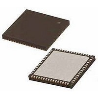
PIC24FJ256GB206-I/MR Microchip Technology, PIC24FJ256GB206-I/MR Datasheet - Page 107

PIC24FJ256GB206-I/MR
Manufacturer Part Number
PIC24FJ256GB206-I/MR
Description
MCU PIC 16BIT FLASH 256K 64VQFN
Manufacturer
Microchip Technology
Series
PIC® 24Fr
Specifications of PIC24FJ256GB206-I/MR
Core Size
16-Bit
Program Memory Size
256KB (85.5K x 24)
Core Processor
PIC
Speed
32MHz
Connectivity
I²C, IrDA, SPI, UART/USART, USB OTG
Peripherals
Brown-out Detect/Reset, LVD, POR, PWM, WDT
Number Of I /o
52
Program Memory Type
FLASH
Ram Size
96K x 8
Voltage - Supply (vcc/vdd)
2.2 V ~ 3.6 V
Data Converters
A/D 16x10b
Oscillator Type
Internal
Operating Temperature
-40°C ~ 85°C
Package / Case
64-VFQFN, Exposed Pad
Controller Family/series
PIC24
No. Of I/o's
52
Ram Memory Size
96KB
Cpu Speed
32MHz
No. Of Timers
5
No. Of Pwm Channels
9
Processor Series
PIC24FJ
Core
PIC
Data Bus Width
16 bit
Data Ram Size
96 KB
Interface Type
I2C, SPI, UART
Maximum Clock Frequency
32 MHz
Number Of Programmable I/os
29
Number Of Timers
5
Operating Supply Voltage
2.2 V to 3.6 V
Maximum Operating Temperature
+ 85 C
Mounting Style
SMD/SMT
3rd Party Development Tools
52713-733, 52714-737, 53276-922, EWDSPIC
Development Tools By Supplier
PG164130, DV164035, DV244005, DV164005, DM240001, MA240021
Minimum Operating Temperature
- 40 C
On-chip Adc
10 bit, 16 Channel
Lead Free Status / RoHS Status
Lead free / RoHS Compliant
Eeprom Size
-
Lead Free Status / Rohs Status
Details
- Current page: 107 of 386
- Download datasheet (4Mb)
REGISTER 7-11:
REGISTER 7-12:
2010 Microchip Technology Inc.
bit 3
bit 2
bit 1
bit 0
bit 15
bit 7
Legend:
R = Readable bit
-n = Value at POR
bit 15
bit 14
bit 13
bit 12
bit 11
bit 10
Note 1:
U2TXIE
R/W-0
R/W-0
IC8IE
If an external interrupt is enabled, the interrupt input must also be configured to an available RPx or RPIx
pin. See Section 10.4 “Peripheral Pin Select (PPS)” for more information.
T1IE: Timer1 Interrupt Enable bit
1 = Interrupt request is enabled
0 = Interrupt request is not enabled
OC1IE: Output Compare Channel 1 Interrupt Enable bit
1 = Interrupt request is enabled
0 = Interrupt request is not enabled
IC1IE: Input Capture Channel 1 Interrupt Enable bit
1 = Interrupt request is enabled
0 = Interrupt request is not enabled
INT0IE: External Interrupt 0 Enable bit
1 = Interrupt request is enabled
0 = Interrupt request is not enabled
U2TXIE: UART2 Transmitter Interrupt Enable bit
1 = Interrupt request is enabled
0 = Interrupt request is not enabled
U2RXIE: UART2 Receiver Interrupt Enable bit
1 = Interrupt request is enabled
0 = Interrupt request is not enabled
INT2IE: External Interrupt 2 Enable bit
1 = Interrupt request is enabled
0 = Interrupt request is not enabled
T5IE: Timer5 Interrupt Enable bit
1 = Interrupt request is enabled
0 = Interrupt request is not enabled
T4IE: Timer4 Interrupt Enable bit
1 = Interrupt request is enabled
0 = Interrupt request is not enabled
OC4IE: Output Compare Channel 4 Interrupt Enable bit
1 = Interrupt request is enabled
0 = Interrupt request is not enabled
U2RXIE
R/W-0
R/W-0
IC7IE
IEC0: INTERRUPT ENABLE CONTROL REGISTER 0 (CONTINUED)
IEC1: INTERRUPT ENABLE CONTROL REGISTER 1
W = Writable bit
‘1’ = Bit is set
INT2IE
R/W-0
U-0
—
(1)
INT1IE
PIC24FJ256GB210 FAMILY
R/W-0
R/W-0
T5IE
(1)
(1)
U = Unimplemented bit, read as ‘0’
‘0’ = Bit is cleared
R/W-0
R/W-0
CNIE
T4IE
OC4IE
R/W-0
R/W-0
CMIE
x = Bit is unknown
MI2C1IE
OC3IE
R/W-0
R/W-0
DS39975A-page 107
SI2C1IE
R/W-0
U-0
—
bit 8
bit 0
Related parts for PIC24FJ256GB206-I/MR
Image
Part Number
Description
Manufacturer
Datasheet
Request
R

Part Number:
Description:
Manufacturer:
Microchip Technology Inc.
Datasheet:

Part Number:
Description:
Manufacturer:
Microchip Technology Inc.
Datasheet:

Part Number:
Description:
Manufacturer:
Microchip Technology Inc.
Datasheet:

Part Number:
Description:
Manufacturer:
Microchip Technology Inc.
Datasheet:

Part Number:
Description:
Manufacturer:
Microchip Technology Inc.
Datasheet:

Part Number:
Description:
Manufacturer:
Microchip Technology Inc.
Datasheet:

Part Number:
Description:
Manufacturer:
Microchip Technology Inc.
Datasheet:

Part Number:
Description:
Manufacturer:
Microchip Technology Inc.
Datasheet:


