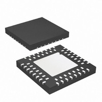
ATMEGA169P-16MCH Atmel, ATMEGA169P-16MCH Datasheet - Page 94

ATMEGA169P-16MCH
Manufacturer Part Number
ATMEGA169P-16MCH
Description
MCU AVR 16KB FLASH 16MHZ 64-VQFN
Manufacturer
Atmel
Series
AVR® ATmegar
Datasheet
1.ATMEGA169PV-8AU.pdf
(395 pages)
Specifications of ATMEGA169P-16MCH
Core Processor
AVR
Core Size
8-Bit
Speed
16MHz
Connectivity
SPI, UART/USART, USI
Peripherals
Brown-out Detect/Reset, LCD, POR, PWM, WDT
Number Of I /o
54
Program Memory Size
16KB (8K x 16)
Program Memory Type
FLASH
Eeprom Size
512 x 8
Ram Size
1K x 8
Voltage - Supply (vcc/vdd)
2.7 V ~ 5.5 V
Data Converters
A/D 8x10b
Oscillator Type
Internal
Operating Temperature
-40°C ~ 85°C
Package / Case
64-VQFN Exposed Pad, 64-HVQFN, 64-SQFN, 64-DHVQFN
For Use With
ATSTK600 - DEV KIT FOR AVR/AVR32ATAVRBFLY - KIT EVALUATION AVR BUTTERFLYATSTK502 - MOD EXPANSION AVR STARTER 500ATSTK500 - PROGRAMMER AVR STARTER KIT
Lead Free Status / RoHS Status
Lead free / RoHS Compliant
- Current page: 94 of 395
- Download datasheet (9Mb)
14.5.1
14.5.2
8018P–AVR–08/10
Force Output Compare
Compare Match Blocking by TCNT0 Write
Figure 14-3. Output Compare Unit, Block Diagram
The OCR0A Register is double buffered when using any of the Pulse Width Modulation (PWM)
modes. For the normal and Clear Timer on Compare (CTC) modes of operation, the double buff-
ering is disabled. The double buffering synchronizes the update of the OCR0 Compare Register
to either top or bottom of the counting sequence. The synchronization prevents the occurrence
of odd-length, non-symmetrical PWM pulses, thereby making the output glitch-free.
The OCR0A Register access may seem complex, but this is not case. When the double buffer-
ing is enabled, the CPU has access to the OCR0A Buffer Register, and if double buffering is
disabled the CPU will access the OCR0A directly.
In non-PWM waveform generation modes, the match output of the comparator can be forced by
writing a one to the Force Output Compare (FOC0A) bit. Forcing compare match will not set the
OCF0A Flag or reload/clear the timer, but the OC0A pin will be updated as if a real compare
match had occurred (the COM0A1:0 bits settings define whether the OC0A pin is set, cleared or
toggled).
All CPU write operations to the TCNT0 Register will block any compare match that occur in the
next timer clock cycle, even when the timer is stopped. This feature allows OCR0A to be initial-
ized to the same value as TCNT0 without triggering an interrupt when the Timer/Counter clock is
enabled.
bottom
FOCn
top
OCRnx
Waveform Generator
WGMn1:0
=
(8-bit Comparator )
DATA BUS
COMnx1:0
TCNTn
OCFnx (Int.Req.)
ATmega169P
OCnx
94
Related parts for ATMEGA169P-16MCH
Image
Part Number
Description
Manufacturer
Datasheet
Request
R

Part Number:
Description:
Manufacturer:
Atmel Corporation
Datasheet:

Part Number:
Description:
Manufacturer:
Atmel Corporation
Datasheet:

Part Number:
Description:
IC AVR MCU 16K 16MHZ IND 64-TQFP
Manufacturer:
Atmel
Datasheet:

Part Number:
Description:
IC AVR MCU 16K 16MHZ IND 64-QFN
Manufacturer:
Atmel
Datasheet:

Part Number:
Description:
MCU AVR 16KB FLASH 16MHZ 64TQFP
Manufacturer:
Atmel
Datasheet:

Part Number:
Description:
MCU AVR 16K ISP FLSH 16MHZ 64QFN
Manufacturer:
Atmel
Datasheet:

Part Number:
Description:
IC MCU AVR 16K 16MHZ IND 64QFN
Manufacturer:
Atmel
Datasheet:

Part Number:
Description:
8-bit Microcontrollers - MCU Microcontroller
Manufacturer:
Atmel

Part Number:
Description:
Atmega169p 8-bit Avr Microcontroller With 16k Bytes In-system Programmable Flash
Manufacturer:
ATMEL Corporation
Datasheet:

Part Number:
Description:
IC AVR MCU 16K 16MHZ IND TQFP
Manufacturer:
Atmel
Datasheet:

Part Number:
Description:
IC AVR MCU 16K 16MHZ IND 64-QFN
Manufacturer:
Atmel
Datasheet:


