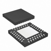
ATMEGA169P-16MCH Atmel, ATMEGA169P-16MCH Datasheet - Page 61

ATMEGA169P-16MCH
Manufacturer Part Number
ATMEGA169P-16MCH
Description
MCU AVR 16KB FLASH 16MHZ 64-VQFN
Manufacturer
Atmel
Series
AVR® ATmegar
Datasheet
1.ATMEGA169PV-8AU.pdf
(395 pages)
Specifications of ATMEGA169P-16MCH
Core Processor
AVR
Core Size
8-Bit
Speed
16MHz
Connectivity
SPI, UART/USART, USI
Peripherals
Brown-out Detect/Reset, LCD, POR, PWM, WDT
Number Of I /o
54
Program Memory Size
16KB (8K x 16)
Program Memory Type
FLASH
Eeprom Size
512 x 8
Ram Size
1K x 8
Voltage - Supply (vcc/vdd)
2.7 V ~ 5.5 V
Data Converters
A/D 8x10b
Oscillator Type
Internal
Operating Temperature
-40°C ~ 85°C
Package / Case
64-VQFN Exposed Pad, 64-HVQFN, 64-SQFN, 64-DHVQFN
For Use With
ATSTK600 - DEV KIT FOR AVR/AVR32ATAVRBFLY - KIT EVALUATION AVR BUTTERFLYATSTK502 - MOD EXPANSION AVR STARTER 500ATSTK500 - PROGRAMMER AVR STARTER KIT
Lead Free Status / RoHS Status
Lead free / RoHS Compliant
- Current page: 61 of 395
- Download datasheet (9Mb)
12. External Interrupts
12.1
8018P–AVR–08/10
Pin Change Interrupt Timing
The External Interrupts are triggered by the INT0 pin or any of the PCINT15..0 pins. Observe
that, if enabled, the interrupts will trigger even if the INT0 or PCINT15..0 pins are configured as
outputs. This feature provides a way of generating a software interrupt. The pin change interrupt
PCI1 will trigger if any enabled PCINT15..8 pin toggles. Pin change interrupts PCI0 will trigger if
any enabled PCINT7..0 pin toggles. The PCMSK1 and PCMSK0 Registers control which pins
contribute to the pin change interrupts. Pin change interrupts on PCINT15..0 are detected asyn-
chronously. This implies that these interrupts can be used for waking the part also from sleep
modes other than Idle mode.
The INT0 interrupts can be triggered by a falling or rising edge or a low level. This is set up as
indicated in the specification for the External Interrupt Control Register A – EICRA. When the
INT0 interrupt is enabled and is configured as level triggered, the interrupt will trigger as long as
the pin is held low. Note that recognition of falling or rising edge interrupts on INT0 requires the
presence of an I/O clock, described in
level interrupt on INT0 is detected asynchronously. This implies that this interrupt can be used
for waking the part also from sleep modes other than Idle mode. The I/O clock is halted in all
sleep modes except Idle mode.
Note that if a level triggered interrupt is used for wake-up from Power-down, the required level
must be held long enough for the MCU to complete the wake-up to trigger the level interrupt. If
the level disappears before the end of the Start-up Time, the MCU will still wake up, but no inter-
rupt will be generated. The start-up time is defined by the SUT and CKSEL Fuses as described
in
An example of timing of a pin change interrupt is shown in
Figure 12-1. Pin Change Interrupt
”System Clock and Clock Options” on page
PCINT(0)
clk
pcint_setflag
pcint_in_(n)
PCINT(n)
pcint_syn
pin_sync
pin_lat
PCIF
clk
LE
pin_lat
D
Q
pin_sync
PCINT(0) in PCMSK(x)
”Clock Systems and their Distribution” on page
pcint_in_(0)
30.
0
x
clk
Figure
pcint_syn
12-1.
ATmega169P
pcint_setflag
PCIF
30. Low
61
Related parts for ATMEGA169P-16MCH
Image
Part Number
Description
Manufacturer
Datasheet
Request
R

Part Number:
Description:
Manufacturer:
Atmel Corporation
Datasheet:

Part Number:
Description:
Manufacturer:
Atmel Corporation
Datasheet:

Part Number:
Description:
IC AVR MCU 16K 16MHZ IND 64-TQFP
Manufacturer:
Atmel
Datasheet:

Part Number:
Description:
IC AVR MCU 16K 16MHZ IND 64-QFN
Manufacturer:
Atmel
Datasheet:

Part Number:
Description:
MCU AVR 16KB FLASH 16MHZ 64TQFP
Manufacturer:
Atmel
Datasheet:

Part Number:
Description:
MCU AVR 16K ISP FLSH 16MHZ 64QFN
Manufacturer:
Atmel
Datasheet:

Part Number:
Description:
IC MCU AVR 16K 16MHZ IND 64QFN
Manufacturer:
Atmel
Datasheet:

Part Number:
Description:
8-bit Microcontrollers - MCU Microcontroller
Manufacturer:
Atmel

Part Number:
Description:
Atmega169p 8-bit Avr Microcontroller With 16k Bytes In-system Programmable Flash
Manufacturer:
ATMEL Corporation
Datasheet:

Part Number:
Description:
IC AVR MCU 16K 16MHZ IND TQFP
Manufacturer:
Atmel
Datasheet:

Part Number:
Description:
IC AVR MCU 16K 16MHZ IND 64-QFN
Manufacturer:
Atmel
Datasheet:


