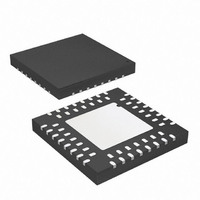
ATMEGA169P-16MCH Atmel, ATMEGA169P-16MCH Datasheet - Page 131

ATMEGA169P-16MCH
Manufacturer Part Number
ATMEGA169P-16MCH
Description
MCU AVR 16KB FLASH 16MHZ 64-VQFN
Manufacturer
Atmel
Series
AVR® ATmegar
Datasheet
1.ATMEGA169PV-8AU.pdf
(395 pages)
Specifications of ATMEGA169P-16MCH
Core Processor
AVR
Core Size
8-Bit
Speed
16MHz
Connectivity
SPI, UART/USART, USI
Peripherals
Brown-out Detect/Reset, LCD, POR, PWM, WDT
Number Of I /o
54
Program Memory Size
16KB (8K x 16)
Program Memory Type
FLASH
Eeprom Size
512 x 8
Ram Size
1K x 8
Voltage - Supply (vcc/vdd)
2.7 V ~ 5.5 V
Data Converters
A/D 8x10b
Oscillator Type
Internal
Operating Temperature
-40°C ~ 85°C
Package / Case
64-VQFN Exposed Pad, 64-HVQFN, 64-SQFN, 64-DHVQFN
For Use With
ATSTK600 - DEV KIT FOR AVR/AVR32ATAVRBFLY - KIT EVALUATION AVR BUTTERFLYATSTK502 - MOD EXPANSION AVR STARTER 500ATSTK500 - PROGRAMMER AVR STARTER KIT
Lead Free Status / RoHS Status
Lead free / RoHS Compliant
- Current page: 131 of 395
- Download datasheet (9Mb)
15.11.3
8018P–AVR–08/10
TCCR1C – Timer/Counter1 Control Register C
When a capture is triggered according to the ICES1 setting, the counter value is copied into the
Input Capture Register (ICR1). The event will also set the Input Capture Flag (ICF1), and this
can be used to cause an Input Capture Interrupt, if this interrupt is enabled.
When the ICR1 is used as TOP value (see description of the WGM13:0 bits located in the
TCCR1A and the TCCR1B Register), the ICP1 is disconnected and consequently the Input Cap-
ture function is disabled.
• Bit 5 – Reserved Bit
This bit is reserved for future use. For ensuring compatibility with future devices, this bit must be
written to zero when TCCR1B is written.
• Bit 4:3 – WGM13:2: Waveform Generation Mode
See TCCR1A Register description.
• Bit 2:0 – CS12:0: Clock Select
The three Clock Select bits select the clock source to be used by the Timer/Counter, see
15-10 on page 126
Table 15-5.
If external pin modes are used for the Timer/Counter1, transitions on the T1 pin will clock the
counter even if the pin is configured as an output. This feature allows software control of the
counting.
• Bit 7 – FOC1A: Force Output Compare for Unit A
• Bit 6 – FOC1B: Force Output Compare for Unit B
The FOC1A/FOC1B bits are only active when the WGM13:0 bits specifies a non-PWM mode.
However, for ensuring compatibility with future devices, these bits must be set to zero when
TCCR1A is written when operating in a PWM mode. When writing a logical one to the
FOC1A/FOC1B bit, an immediate compare match is forced on the Waveform Generation unit.
The OC1A/OC1B output is changed according to its COM1x1:0 bits setting. Note that the
Bit
(0x82)
Read/Write
Initial Value
CS12
0
0
0
0
1
1
1
1
CS11
0
0
1
1
0
0
1
1
Clock Select Bit Description
FOC1A
R/W
7
0
and
CS10
Figure 15-11 on page
FOC1B
0
1
0
1
0
1
0
1
R/W
6
0
Description
No clock source (Timer/Counter stopped).
clk
clk
clk
clk
clk
External clock source on T1 pin. Clock on falling edge.
External clock source on T1 pin. Clock on rising edge.
I/O
I/O
I/O
I/O
I/O
R
5
–
0
/1 (No prescaling)
/8 (From prescaler)
/64 (From prescaler)
/256 (From prescaler)
/1024 (From prescaler)
R
4
–
0
126.
R
3
–
0
R
2
–
0
ATmega169P
R
1
–
0
R
0
–
0
TCCR1C
Figure
131
Related parts for ATMEGA169P-16MCH
Image
Part Number
Description
Manufacturer
Datasheet
Request
R

Part Number:
Description:
Manufacturer:
Atmel Corporation
Datasheet:

Part Number:
Description:
Manufacturer:
Atmel Corporation
Datasheet:

Part Number:
Description:
IC AVR MCU 16K 16MHZ IND 64-TQFP
Manufacturer:
Atmel
Datasheet:

Part Number:
Description:
IC AVR MCU 16K 16MHZ IND 64-QFN
Manufacturer:
Atmel
Datasheet:

Part Number:
Description:
MCU AVR 16KB FLASH 16MHZ 64TQFP
Manufacturer:
Atmel
Datasheet:

Part Number:
Description:
MCU AVR 16K ISP FLSH 16MHZ 64QFN
Manufacturer:
Atmel
Datasheet:

Part Number:
Description:
IC MCU AVR 16K 16MHZ IND 64QFN
Manufacturer:
Atmel
Datasheet:

Part Number:
Description:
8-bit Microcontrollers - MCU Microcontroller
Manufacturer:
Atmel

Part Number:
Description:
Atmega169p 8-bit Avr Microcontroller With 16k Bytes In-system Programmable Flash
Manufacturer:
ATMEL Corporation
Datasheet:

Part Number:
Description:
IC AVR MCU 16K 16MHZ IND TQFP
Manufacturer:
Atmel
Datasheet:

Part Number:
Description:
IC AVR MCU 16K 16MHZ IND 64-QFN
Manufacturer:
Atmel
Datasheet:


