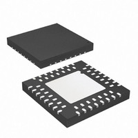
ATMEGA169P-16MCH Atmel, ATMEGA169P-16MCH Datasheet - Page 173

ATMEGA169P-16MCH
Manufacturer Part Number
ATMEGA169P-16MCH
Description
MCU AVR 16KB FLASH 16MHZ 64-VQFN
Manufacturer
Atmel
Series
AVR® ATmegar
Datasheet
1.ATMEGA169PV-8AU.pdf
(395 pages)
Specifications of ATMEGA169P-16MCH
Core Processor
AVR
Core Size
8-Bit
Speed
16MHz
Connectivity
SPI, UART/USART, USI
Peripherals
Brown-out Detect/Reset, LCD, POR, PWM, WDT
Number Of I /o
54
Program Memory Size
16KB (8K x 16)
Program Memory Type
FLASH
Eeprom Size
512 x 8
Ram Size
1K x 8
Voltage - Supply (vcc/vdd)
2.7 V ~ 5.5 V
Data Converters
A/D 8x10b
Oscillator Type
Internal
Operating Temperature
-40°C ~ 85°C
Package / Case
64-VQFN Exposed Pad, 64-HVQFN, 64-SQFN, 64-DHVQFN
For Use With
ATSTK600 - DEV KIT FOR AVR/AVR32ATAVRBFLY - KIT EVALUATION AVR BUTTERFLYATSTK502 - MOD EXPANSION AVR STARTER 500ATSTK500 - PROGRAMMER AVR STARTER KIT
Lead Free Status / RoHS Status
Lead free / RoHS Compliant
- Current page: 173 of 395
- Download datasheet (9Mb)
19.3.4
19.4
8018P–AVR–08/10
Frame Formats
Synchronous Clock Operation
When synchronous mode is used (UMSELn = 1), the XCK pin will be used as either clock input
(Slave) or clock output (Master). The dependency between the clock edges and data sampling
or data change is the same. The basic principle is that data input (on RxD) is sampled at the
opposite XCK clock edge of the edge the data output (TxD) is changed.
Figure 19-3. Synchronous Mode XCK Timing.
The UCPOLn bit UCRSC selects which XCK clock edge is used for data sampling and which is
used for data change. As
rising XCK edge and sampled at falling XCK edge. If UCPOLn is set, the data will be changed at
falling XCK edge and sampled at rising XCK edge.
A serial frame is defined to be one character of data bits with synchronization bits (start and stop
bits), and optionally a parity bit for error checking. The USART accepts all 30 combinations of
the following as valid frame formats:
• 1 start bit
• 5, 6, 7, 8, or 9 data bits
• no, even or odd parity bit
• 1 or 2 stop bits
A frame starts with the start bit followed by the least significant data bit. Then the next data bits,
up to a total of nine, are succeeding, ending with the most significant bit. If enabled, the parity bit
is inserted after the data bits, before the stop bits. When a complete frame is transmitted, it can
be directly followed by a new frame, or the communication line can be set to an idle (high) state.
Figure 19-4 on page 174
brackets are optional.
UCPOL = 1
UCPOL = 0
RxD / TxD
RxD / TxD
XCK
XCK
Figure 19-3
illustrates the possible combinations of the frame formats. Bits inside
shows, when UCPOLn is zero the data will be changed at
Sample
Sample
ATmega169P
173
Related parts for ATMEGA169P-16MCH
Image
Part Number
Description
Manufacturer
Datasheet
Request
R

Part Number:
Description:
Manufacturer:
Atmel Corporation
Datasheet:

Part Number:
Description:
Manufacturer:
Atmel Corporation
Datasheet:

Part Number:
Description:
IC AVR MCU 16K 16MHZ IND 64-TQFP
Manufacturer:
Atmel
Datasheet:

Part Number:
Description:
IC AVR MCU 16K 16MHZ IND 64-QFN
Manufacturer:
Atmel
Datasheet:

Part Number:
Description:
MCU AVR 16KB FLASH 16MHZ 64TQFP
Manufacturer:
Atmel
Datasheet:

Part Number:
Description:
MCU AVR 16K ISP FLSH 16MHZ 64QFN
Manufacturer:
Atmel
Datasheet:

Part Number:
Description:
IC MCU AVR 16K 16MHZ IND 64QFN
Manufacturer:
Atmel
Datasheet:

Part Number:
Description:
8-bit Microcontrollers - MCU Microcontroller
Manufacturer:
Atmel

Part Number:
Description:
Atmega169p 8-bit Avr Microcontroller With 16k Bytes In-system Programmable Flash
Manufacturer:
ATMEL Corporation
Datasheet:

Part Number:
Description:
IC AVR MCU 16K 16MHZ IND TQFP
Manufacturer:
Atmel
Datasheet:

Part Number:
Description:
IC AVR MCU 16K 16MHZ IND 64-QFN
Manufacturer:
Atmel
Datasheet:


