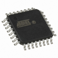
ATTINY28L-4AU Atmel, ATTINY28L-4AU Datasheet - Page 47

ATTINY28L-4AU
Manufacturer Part Number
ATTINY28L-4AU
Description
IC MCU AVR 2K FLASH 4MHZ 32-TQFP
Manufacturer
Atmel
Series
AVR® ATtinyr
Specifications of ATTINY28L-4AU
Core Processor
AVR
Core Size
8-Bit
Speed
4MHz
Peripherals
POR, WDT
Number Of I /o
11
Program Memory Size
2KB (1K x 16)
Program Memory Type
FLASH
Voltage - Supply (vcc/vdd)
2.7 V ~ 5.5 V
Oscillator Type
Internal
Operating Temperature
-40°C ~ 85°C
Package / Case
32-TQFP, 32-VQFP
Processor Series
ATTINY2x
Core
AVR8
Data Bus Width
8 bit
Data Ram Size
32 B
Maximum Clock Frequency
4 MHz
Number Of Programmable I/os
11
Number Of Timers
1
Maximum Operating Temperature
+ 85 C
Mounting Style
SMD/SMT
3rd Party Development Tools
EWAVR, EWAVR-BL
Development Tools By Supplier
ATAVRDRAGON, ATSTK500, ATSTK600, ATAVRISP2, ATAVRONEKIT
Minimum Operating Temperature
- 40 C
On-chip Adc
8 bit
Package
32TQFP
Device Core
AVR
Family Name
ATtiny
Maximum Speed
4 MHz
Ram Size
32 Byte
Operating Supply Voltage
3.3|5 V
For Use With
ATSTK600-DIP40 - STK600 SOCKET/ADAPTER 40-PDIPATSTK500 - PROGRAMMER AVR STARTER KIT
Lead Free Status / RoHS Status
Lead free / RoHS Compliant
Eeprom Size
-
Ram Size
-
Data Converters
-
Connectivity
-
Lead Free Status / Rohs Status
Details
Available stocks
Company
Part Number
Manufacturer
Quantity
Price
Programming the Flash
Parallel Programming
Signal Names
1062F–AVR–07/06
Atmel’s ATtiny28 offers 2K bytes of Flash program memory.
The ATtiny28 is shipped with the on-chip Flash program memory array in the erased
state (i.e., contents = $FF) and ready to be programmed. This device supports a high-
voltage (12V) parallel programming mode. Only minor currents (<1mA) are drawn from
the +12V pin during programming.
The program memory array in the ATtiny28 is programmed byte-by-byte. During pro-
gramming, the supply voltage must be in accordance with Table 21.
Table 21. Supply Voltage during Programming
This section describes how to parallel program and verify Flash program memory, Lock
bits and Fuse bits in the ATtiny28.
In this section, some pins of the ATtiny28 are referenced by signal names describing
their function during parallel programming. See Figure 37 and Table 22. Pins not
described in Table 22 are referenced by pin name.
The XA1/XA0 pins determine the action executed when the XTAL1 pin is given a posi-
tive pulse. The coding is shown in Table 23.
When pulsing WR or OE, the command loaded determines the action executed. The
command is a byte where the different bits are assigned functions, as shown in Table
24.
Figure 37. Parallel Programming
Part
ATtiny28
RDY/BSY
Serial Programming
Not applicable
+12V
XA0
XA1
WR
OE
BS
PD1
PD2
PD3
PD4
PD5
PD6
RESET
XTAL1
GND
ATtiny28
PB7 - PB0
VCC
Parallel Programming
4.5 - 5.5V
+5V
ATtiny28L/V
DATA
47


