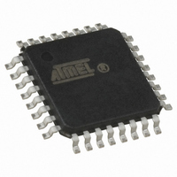
ATTINY28L-4AU Atmel, ATTINY28L-4AU Datasheet - Page 43

ATTINY28L-4AU
Manufacturer Part Number
ATTINY28L-4AU
Description
IC MCU AVR 2K FLASH 4MHZ 32-TQFP
Manufacturer
Atmel
Series
AVR® ATtinyr
Specifications of ATTINY28L-4AU
Core Processor
AVR
Core Size
8-Bit
Speed
4MHz
Peripherals
POR, WDT
Number Of I /o
11
Program Memory Size
2KB (1K x 16)
Program Memory Type
FLASH
Voltage - Supply (vcc/vdd)
2.7 V ~ 5.5 V
Oscillator Type
Internal
Operating Temperature
-40°C ~ 85°C
Package / Case
32-TQFP, 32-VQFP
Processor Series
ATTINY2x
Core
AVR8
Data Bus Width
8 bit
Data Ram Size
32 B
Maximum Clock Frequency
4 MHz
Number Of Programmable I/os
11
Number Of Timers
1
Maximum Operating Temperature
+ 85 C
Mounting Style
SMD/SMT
3rd Party Development Tools
EWAVR, EWAVR-BL
Development Tools By Supplier
ATAVRDRAGON, ATSTK500, ATSTK600, ATAVRISP2, ATAVRONEKIT
Minimum Operating Temperature
- 40 C
On-chip Adc
8 bit
Package
32TQFP
Device Core
AVR
Family Name
ATtiny
Maximum Speed
4 MHz
Ram Size
32 Byte
Operating Supply Voltage
3.3|5 V
For Use With
ATSTK600-DIP40 - STK600 SOCKET/ADAPTER 40-PDIPATSTK500 - PROGRAMMER AVR STARTER KIT
Lead Free Status / RoHS Status
Lead free / RoHS Compliant
Eeprom Size
-
Ram Size
-
Data Converters
-
Connectivity
-
Lead Free Status / Rohs Status
Details
Available stocks
Company
Part Number
Manufacturer
Quantity
Price
Register Description
Modulation Control Register –
MODCR
Table 18. MCONF2..0 Effect on Duty-cycle and Modulation Period
Note:
1062F–AVR–07/06
MCONF2..0
000
001
010
011
100
101
110
111
In the high-frequency mode, the output is gated with the clock signal. Thus, the on- and off-times will be dependent on the clock
input to the MCU. Also note that when changing from this mode directly to another modulation mode, the output will have a
small glitch. Thus, PA2 should be set to stop the modulated output before changing from this mode.
On-time
X
ONTIM+1
ONTIM+1
ONTIM+1
2 x (ONTIM+1)
3 x (ONTIM+1)
X
Off-time
X
ONTIM+1
2 x (ONTIM+1)
3 x (ONTIM+1)
ONTIM+1
ONTIM+1
X
• Bits 7..3 – ONTIM4..0: Modulation On-time
This 5-bit value +1 determines the number of clock cycles the output pin PA2 is active
(low).
• Bits 2..0 – MCONF2..0: Modulation Configuration Bits 2, 1 and 0
These three bits determine the relationship between the on- and off-times of the modu-
lator, and thereby the duty-cycle. The various settings are shown in Table 18. The
minimum and maximum modulation period is also shown in the table. The minimum
modulation period is obtained by setting ONTIM to zero, while the maximum period is
obtained by setting ONTIM to 31. The configuration values for some common oscillator
and carrier frequencies are listed in Table 17. The relationship between oscillator fre-
quency and carrier frequency is:
If the MCONF register is set to 111, the carrier frequency will be equal to the oscillator
frequency.
Bit
$02
Read/Write
Initial Value
ONTIM4
R/W
7
0
Duty-cycle
100%
50%
33%
25%
67%
75%
Note 1
ONTIM3
R/W
6
0
fcarrier
ONTIM2
Reserved
R/W
5
0
Min Period
X
2 CK
3 CK
4 CK
3 CK
4 CK
1 CK
=
-----------------------------------------------------
(
On-time
ONTIM1
R/W
4
0
fosc
+
ONTIM0
R/W
Off-time
3
0
Max Period
X
64 CK
96 CK
128 CK
96 CK
128 CK
1 CK
MCONF2
R/W
)
2
0
MCONF1
ATtiny28L/V
R/W
1
0
Comment
Unmodulated output
High-frequency output
MCONF0
R/W
0
0
MODCR
43


