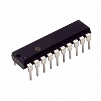
PIC16C770-I/P Microchip Technology, PIC16C770-I/P Datasheet - Page 110

PIC16C770-I/P
Manufacturer Part Number
PIC16C770-I/P
Description
IC MCU CMOS A/D 2K 20MHZ 20-DIP
Manufacturer
Microchip Technology
Series
PIC® 16Cr
Datasheets
1.PIC16C770-ISO.pdf
(220 pages)
2.PIC16C770-ISO.pdf
(6 pages)
3.PIC16C770-ISO.pdf
(8 pages)
Specifications of PIC16C770-I/P
Core Size
8-Bit
Program Memory Size
3.5KB (2K x 14)
Oscillator Type
Internal
Core Processor
PIC
Speed
20MHz
Connectivity
I²C, SPI
Peripherals
Brown-out Detect/Reset, POR, PWM, WDT
Number Of I /o
15
Program Memory Type
OTP
Ram Size
256 x 8
Voltage - Supply (vcc/vdd)
4 V ~ 5.5 V
Data Converters
A/D 6x12b
Operating Temperature
-40°C ~ 85°C
Package / Case
20-DIP (0.300", 7.62mm)
Controller Family/series
PIC16C
No. Of I/o's
16
Ram Memory Size
256Byte
Cpu Speed
20MHz
No. Of Timers
3
No. Of
RoHS Compliant
Core
PIC
Processor Series
PIC16C
Data Bus Width
8 bit
Maximum Clock Frequency
20 MHz
Data Ram Size
256 B
Data Rom Size
256 B
On-chip Adc
6 bit
Number Of Programmable I/os
16
Number Of Timers
3 bit
Operating Supply Voltage
2.5 V to 5.5 V
Mounting Style
Through Hole
Height
3.3 mm
Interface Type
I2C, SPI, SSP
Length
26.16 mm
Maximum Operating Temperature
+ 85 C
Minimum Operating Temperature
- 40 C
Supply Voltage (max)
5.5 V
Supply Voltage (min)
4 V
Width
6.35 mm
Lead Free Status / RoHS Status
Lead free / RoHS Compliant
For Use With
DVA16XP200 - ADAPTER ICE 20DIP/SOIC/SSOPAC164028 - MODULE SKT PROMATEII 20SOIC/DIP
Eeprom Size
-
Lead Free Status / Rohs Status
Details
Other names
PIC16C770I/P
- Current page: 110 of 220
- Download datasheet (4Mb)
PIC16C717/770/771
FIGURE 11-2: PIC16C717 10-BIT A/D RESULT FORMAT
After the A/D module has been configured as desired,
the selected channel must be acquired before the con-
version is started. The analog input channels must
have their corresponding TRIS and ANSEL bits
selected as an input. To determine acquisition time, see
Section 11.6. After this acquisition time has elapsed,
the A/D conversion can be started. The following steps
should be followed for doing an A/D conversion:
11.2
11.2.1
The ANSEL and TRIS registers control the operation
of the A/D port pins. The port pins that are desired as
analog inputs must have their corresponding TRIS bit
set (input). If the TRIS bit is cleared (output), the digital
output level (V
ANSEL bits must be set (analog input) to disable the
digital input buffer.
The A/D operation is independent of the state of the
TRIS bits and the ANSEL bits.
DS41120B-page 108
Note 1: When reading the PORTA register, all pins
(ADFM = 0)
(ADFM = 1)
3: Analog levels on any pin that is defined as
Configuring the A/D Module
2: When reading the PORTB register, all
CONFIGURING ANALOG PORT
PINS
configured as analog input channels will
read as ’0’.
a digital input, including the ANx pins, may
cause the input buffer to consume current
that is out of the devices specification.
pins configured as analog pins on
PORTB will be read as ’1’.
OH
or V
OL
MSB
bit7
bit7
) will be converted. The proper
Unused
10-bit A/D Result
MSB
11.2.2
The VCFG bits in the ADCON1 register configure the
A/D module reference inputs. The reference high input
can come from an internal reference (VRH) or (VRL),
an external reference (V
ence input can come from an internal reference (VRL),
an external reference (V
reference is chosen for the reference high or reference
low inputs, the port pin that multiplexes the incoming
external references is configured as an analog input,
regardless of the values contained in the A/D port con-
figuration bits (PCFG<3:0>).
10-bit A/D Result
bit7
bit7
CONFIGURING THE REFERENCE
VOLTAGES
LSB
REF
REF
2002 Microchip Technology Inc.
+), or AV
-), or AV
Unused
LSB
DD
SS
. The low refer-
. If an external
Unused
Related parts for PIC16C770-I/P
Image
Part Number
Description
Manufacturer
Datasheet
Request
R

Part Number:
Description:
IC MCU OTP 8KX14 A/D PWM 44PLCC
Manufacturer:
Microchip Technology
Datasheet:

Part Number:
Description:
IC MCU OTP 8KX14 A/D PWM 44PLCC
Manufacturer:
Microchip Technology
Datasheet:

Part Number:
Description:
IC MCU OTP 8KX14 A/D PWM 44TQFP
Manufacturer:
Microchip Technology
Datasheet:

Part Number:
Description:
IC MCU OTP 8KX14 A/D PWM 44-MQFP
Manufacturer:
Microchip Technology
Datasheet:

Part Number:
Description:
IC MCU OTP 8KX14 A/D PWM 40DIP
Manufacturer:
Microchip Technology
Datasheet:

Part Number:
Description:
IC MCU OTP 8KX14 A/D PWM 44PLCC
Manufacturer:
Microchip Technology
Datasheet:

Part Number:
Description:
IC MCU OTP 8KX14 A/D PWM 40DIP
Manufacturer:
Microchip Technology
Datasheet:

Part Number:
Description:
IC MCU OTP 8KX14 A/D PWM 40DIP
Manufacturer:
Microchip Technology
Datasheet:

Part Number:
Description:
IC MCU OTP 8KX14 A/D PWM 40DIP
Manufacturer:
Microchip Technology
Datasheet:

Part Number:
Description:
IC MCU OTP 8KX14 A/D PWM 44PLCC
Manufacturer:
Microchip Technology
Datasheet:

Part Number:
Description:
IC MCU OTP 8KX14 A/D PWM 44PLCC
Manufacturer:
Microchip Technology
Datasheet:

Part Number:
Description:
IC MCU OTP 8KX14 A/D PWM 44-MQFP
Manufacturer:
Microchip Technology
Datasheet:

Part Number:
Description:
IC MCU OTP 8KX14 A/D PWM 40DIP
Manufacturer:
Microchip Technology
Datasheet:

Part Number:
Description:
IC MCU OTP 8KX14 A/D PWM 44-MQFP
Manufacturer:
Microchip Technology
Datasheet:

Part Number:
Description:
IC MCU OTP 8KX14 A/D PWM 40DIP
Manufacturer:
Microchip Technology
Datasheet:


