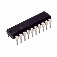
PIC16C770-I/P Microchip Technology, PIC16C770-I/P Datasheet - Page 107

PIC16C770-I/P
Manufacturer Part Number
PIC16C770-I/P
Description
IC MCU CMOS A/D 2K 20MHZ 20-DIP
Manufacturer
Microchip Technology
Series
PIC® 16Cr
Datasheets
1.PIC16C770-ISO.pdf
(220 pages)
2.PIC16C770-ISO.pdf
(6 pages)
3.PIC16C770-ISO.pdf
(8 pages)
Specifications of PIC16C770-I/P
Core Size
8-Bit
Program Memory Size
3.5KB (2K x 14)
Oscillator Type
Internal
Core Processor
PIC
Speed
20MHz
Connectivity
I²C, SPI
Peripherals
Brown-out Detect/Reset, POR, PWM, WDT
Number Of I /o
15
Program Memory Type
OTP
Ram Size
256 x 8
Voltage - Supply (vcc/vdd)
4 V ~ 5.5 V
Data Converters
A/D 6x12b
Operating Temperature
-40°C ~ 85°C
Package / Case
20-DIP (0.300", 7.62mm)
Controller Family/series
PIC16C
No. Of I/o's
16
Ram Memory Size
256Byte
Cpu Speed
20MHz
No. Of Timers
3
No. Of
RoHS Compliant
Core
PIC
Processor Series
PIC16C
Data Bus Width
8 bit
Maximum Clock Frequency
20 MHz
Data Ram Size
256 B
Data Rom Size
256 B
On-chip Adc
6 bit
Number Of Programmable I/os
16
Number Of Timers
3 bit
Operating Supply Voltage
2.5 V to 5.5 V
Mounting Style
Through Hole
Height
3.3 mm
Interface Type
I2C, SPI, SSP
Length
26.16 mm
Maximum Operating Temperature
+ 85 C
Minimum Operating Temperature
- 40 C
Supply Voltage (max)
5.5 V
Supply Voltage (min)
4 V
Width
6.35 mm
Lead Free Status / RoHS Status
Lead free / RoHS Compliant
For Use With
DVA16XP200 - ADAPTER ICE 20DIP/SOIC/SSOPAC164028 - MODULE SKT PROMATEII 20SOIC/DIP
Eeprom Size
-
Lead Free Status / Rohs Status
Details
Other names
PIC16C770I/P
- Current page: 107 of 220
- Download datasheet (4Mb)
11.0
The analog-to-digital (A/D) converter module has six
inputs for the PIC16C717/770/771.
The PIC16C717 analog-to-digital converter (A/D)
allows conversion of an analog input signal to a corre-
sponding 10-bit digital value, while the A/D converter
in the PIC16C770/771 allows conversion to a corre-
sponding 12-bit digital value. The A/D module has up
to 6 analog inputs, which are multiplexed into one
sample and hold. The output of the sample and hold is
the input into the converter, which generates the result
via successive approximation. The analog reference
voltages are software selectable to either the device’s
analog positive and negative supply voltages (AV
AV
or internal voltage references if enabled (VRH, VRL).
The A/D converter can be triggered by setting the GO/
DONE bit, or by the special event Compare mode of
the ECCP module. When conversion is complete, the
GO/DONE bit returns to ’0’, the ADIF bit in the PIR1
register is set, and an A/D interrupt will occur, if
enabled.
The A/D converter has a unique feature of being able
to operate while the device is in SLEEP mode. To oper-
ate in SLEEP, the A/D conversion clock must be
derived from the A/D’s internal RC oscillator.
2002 Microchip Technology Inc.
SS
), the voltage level on the V
ANALOG-TO-DIGITAL
CONVERTER (A/D) MODULE
REF
+ and V
REF
- pins,
DD
/
The A/D module has four registers. These registers
are:
A device RESET forces all registers to their RESET
state. This forces the A/D module to be turned off and
any conversion is aborted.
11.1
The ADCON0 register, shown in Register 11-1, con-
trols the operation of the A/D module. The ADCON1
register, shown in Register 11-2, configures the func-
tions of the port pins, the voltage reference configura-
tion and the result format. The ANSEL register, shown
in Register 3-1, selects between the Analog or Digital
Port Pin modes. The port pins can be configured as
analog inputs or as digital I/O.
The combination of the ADRESH and ADRESL regis-
ters contain the result of the A/D conversion. The reg-
ister pair is referred to as the ADRES register. When
the A/D conversion is complete, the result is loaded
into ADRES, the GO/DONE bit (ADCON0<2>) is
cleared, and the A/D interrupt flag ADIF is set. The
block diagram of the A/D module is shown in
Figure 11-3.
PIC16C717/770/771
• A/D Result Register Low ADRESL
• A/D Result Register High ADRESH
• A/D Control Register 0 (ADCON0)
• A/D Control Register 1 (ADCON1)
Control Registers
DS41120B-page 105
Related parts for PIC16C770-I/P
Image
Part Number
Description
Manufacturer
Datasheet
Request
R

Part Number:
Description:
IC MCU OTP 8KX14 A/D PWM 44PLCC
Manufacturer:
Microchip Technology
Datasheet:

Part Number:
Description:
IC MCU OTP 8KX14 A/D PWM 44PLCC
Manufacturer:
Microchip Technology
Datasheet:

Part Number:
Description:
IC MCU OTP 8KX14 A/D PWM 44TQFP
Manufacturer:
Microchip Technology
Datasheet:

Part Number:
Description:
IC MCU OTP 8KX14 A/D PWM 44-MQFP
Manufacturer:
Microchip Technology
Datasheet:

Part Number:
Description:
IC MCU OTP 8KX14 A/D PWM 40DIP
Manufacturer:
Microchip Technology
Datasheet:

Part Number:
Description:
IC MCU OTP 8KX14 A/D PWM 44PLCC
Manufacturer:
Microchip Technology
Datasheet:

Part Number:
Description:
IC MCU OTP 8KX14 A/D PWM 40DIP
Manufacturer:
Microchip Technology
Datasheet:

Part Number:
Description:
IC MCU OTP 8KX14 A/D PWM 40DIP
Manufacturer:
Microchip Technology
Datasheet:

Part Number:
Description:
IC MCU OTP 8KX14 A/D PWM 40DIP
Manufacturer:
Microchip Technology
Datasheet:

Part Number:
Description:
IC MCU OTP 8KX14 A/D PWM 44PLCC
Manufacturer:
Microchip Technology
Datasheet:

Part Number:
Description:
IC MCU OTP 8KX14 A/D PWM 44PLCC
Manufacturer:
Microchip Technology
Datasheet:

Part Number:
Description:
IC MCU OTP 8KX14 A/D PWM 44-MQFP
Manufacturer:
Microchip Technology
Datasheet:

Part Number:
Description:
IC MCU OTP 8KX14 A/D PWM 40DIP
Manufacturer:
Microchip Technology
Datasheet:

Part Number:
Description:
IC MCU OTP 8KX14 A/D PWM 44-MQFP
Manufacturer:
Microchip Technology
Datasheet:

Part Number:
Description:
IC MCU OTP 8KX14 A/D PWM 40DIP
Manufacturer:
Microchip Technology
Datasheet:


