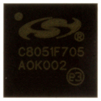
C8051F705-GM Silicon Laboratories Inc, C8051F705-GM Datasheet - Page 47

C8051F705-GM
Manufacturer Part Number
C8051F705-GM
Description
IC 8051 MCU 15K FLASH 48-QFN
Manufacturer
Silicon Laboratories Inc
Series
C8051F70xr
Specifications of C8051F705-GM
Core Processor
8051
Core Size
8-Bit
Speed
25MHz
Connectivity
SMBus (2-Wire/I²C), SPI, UART/USART
Peripherals
Cap Sense, POR, PWM, WDT
Number Of I /o
39
Program Memory Size
15KB (15K x 8)
Program Memory Type
FLASH
Eeprom Size
32 x 8
Ram Size
512 x 8
Voltage - Supply (vcc/vdd)
1.8 V ~ 3.6 V
Oscillator Type
Internal
Operating Temperature
-40°C ~ 85°C
Package / Case
48-QFN
Processor Series
C8051F7x
Core
8051
Data Bus Width
8 bit
Data Ram Size
512 B
Interface Type
I2C, SMBus, SPI, UART
Maximum Clock Frequency
25 MHz
Number Of Programmable I/os
39
Number Of Timers
4
Maximum Operating Temperature
+ 85 C
Mounting Style
SMD/SMT
3rd Party Development Tools
PK51, CA51, A51, ULINK2
Development Tools By Supplier
C8051F700DK
Minimum Operating Temperature
- 40 C
Height
0.95 mm
Length
7 mm
Supply Voltage (max)
1.9 V, 3.6 V
Supply Voltage (min)
1.7 V, 1.8 V
Width
7 mm
For Use With
336-1635 - DEV KIT FOR C8051F700
Lead Free Status / RoHS Status
Lead free / RoHS Compliant
Data Converters
-
Lead Free Status / Rohs Status
Details
Other names
336-1612-5
Available stocks
Company
Part Number
Manufacturer
Quantity
Price
Company:
Part Number:
C8051F705-GM
Manufacturer:
Silicon Laboratories Inc
Quantity:
135
- Current page: 47 of 306
- Download datasheet (2Mb)
9. Electrical Characteristics
9.1. Absolute Maximum Specifications
Table 9.1. Absolute Maximum Ratings
Parameter
Ambient temperature under bias
Storage Temperature
Voltage on RST or any Port I/O Pin
(except P0.3) with respect to GND
Voltage on P0.3 with respect to GND
Voltage on V
Maximum Total current through V
and GND
Maximum output current sunk by RST
or any Port pin
Note: Stresses above those listed under “Absolute Maximum Ratings” may cause permanent damage to the device.
This is a stress rating only and functional operation of the devices at those or any other conditions above
those indicated in the operation listings of this specification is not implied. Exposure to maximum rating
conditions for extended periods may affect device reliability.
DD
with respect to GND
DD
Regulator in Bypass Mode
Regulator in Normal Mode
Conditions
Rev. 1.0
–0.3
–0.3
–0.3
–0.3
Min
–55
–65
—
—
C8051F70x/71x
Typ
—
—
—
—
—
—
—
—
V
V
DD
DD
Max
1.98
125
150
500
100
4.2
+ 2.0
+ 0.3
Units
mA
mA
°C
°C
V
V
V
V
47
Related parts for C8051F705-GM
Image
Part Number
Description
Manufacturer
Datasheet
Request
R
Part Number:
Description:
SMD/C°/SINGLE-ENDED OUTPUT SILICON OSCILLATOR
Manufacturer:
Silicon Laboratories Inc
Part Number:
Description:
Manufacturer:
Silicon Laboratories Inc
Datasheet:
Part Number:
Description:
N/A N/A/SI4010 AES KEYFOB DEMO WITH LCD RX
Manufacturer:
Silicon Laboratories Inc
Datasheet:
Part Number:
Description:
N/A N/A/SI4010 SIMPLIFIED KEY FOB DEMO WITH LED RX
Manufacturer:
Silicon Laboratories Inc
Datasheet:
Part Number:
Description:
N/A/-40 TO 85 OC/EZLINK MODULE; F930/4432 HIGH BAND (REV E/B1)
Manufacturer:
Silicon Laboratories Inc
Part Number:
Description:
EZLink Module; F930/4432 Low Band (rev e/B1)
Manufacturer:
Silicon Laboratories Inc
Part Number:
Description:
I°/4460 10 DBM RADIO TEST CARD 434 MHZ
Manufacturer:
Silicon Laboratories Inc
Part Number:
Description:
I°/4461 14 DBM RADIO TEST CARD 868 MHZ
Manufacturer:
Silicon Laboratories Inc
Part Number:
Description:
I°/4463 20 DBM RFSWITCH RADIO TEST CARD 460 MHZ
Manufacturer:
Silicon Laboratories Inc
Part Number:
Description:
I°/4463 20 DBM RADIO TEST CARD 868 MHZ
Manufacturer:
Silicon Laboratories Inc
Part Number:
Description:
I°/4463 27 DBM RADIO TEST CARD 868 MHZ
Manufacturer:
Silicon Laboratories Inc
Part Number:
Description:
I°/4463 SKYWORKS 30 DBM RADIO TEST CARD 915 MHZ
Manufacturer:
Silicon Laboratories Inc
Part Number:
Description:
N/A N/A/-40 TO 85 OC/4463 RFMD 30 DBM RADIO TEST CARD 915 MHZ
Manufacturer:
Silicon Laboratories Inc
Part Number:
Description:
I°/4463 20 DBM RADIO TEST CARD 169 MHZ
Manufacturer:
Silicon Laboratories Inc


