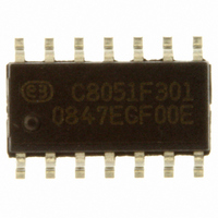
C8051F301-GS Silicon Laboratories Inc, C8051F301-GS Datasheet - Page 91

C8051F301-GS
Manufacturer Part Number
C8051F301-GS
Description
IC 8051 MCU 8K FLASH 14-SOIC
Manufacturer
Silicon Laboratories Inc
Series
C8051F30xr
Specifications of C8051F301-GS
Program Memory Type
FLASH
Program Memory Size
8KB (8K x 8)
Package / Case
14-SOIC (3.9mm Width), 14-SOL
Core Processor
8051
Core Size
8-Bit
Speed
25MHz
Connectivity
SMBus (2-Wire/I²C), UART/USART
Peripherals
POR, PWM, WDT
Number Of I /o
8
Ram Size
256 x 8
Voltage - Supply (vcc/vdd)
2.7 V ~ 3.6 V
Oscillator Type
Internal
Operating Temperature
-40°C ~ 85°C
Processor Series
C8051F3x
Core
8051
Data Bus Width
8 bit
Data Ram Size
256 B
Interface Type
I2C/SMBus/UART
Maximum Clock Frequency
25 MHz
Number Of Programmable I/os
8
Number Of Timers
3
Maximum Operating Temperature
+ 85 C
Mounting Style
SMD/SMT
3rd Party Development Tools
PK51, CA51, A51, ULINK2
Development Tools By Supplier
C8051F300DK
Minimum Operating Temperature
- 40 C
Package
14SOIC
Device Core
8051
Family Name
C8051F30x
Maximum Speed
25 MHz
Operating Supply Voltage
3.3 V
Lead Free Status / RoHS Status
Lead free / RoHS Compliant
For Use With
770-1006 - ISP 4PORT FOR SILABS C8051F MCU336-1444 - ADAPTER PROGRAM TOOLSTICK F300336-1319 - REFERENCE DESIGN STEPPER MOTOR
Eeprom Size
-
Data Converters
-
Lead Free Status / Rohs Status
Lead free / RoHS Compliant
Other names
336-1536-5
The lock bits can always be read and cleared to logic 0 regardless of the security settings.
Important note: The only means of removing a lock (write or read/write) once set is to erase the
entire program memory space via a C2 Device Erase command.
The level of Flash security depends on the Flash access method. The three Flash access methods that
can be restricted are reads, writes, and erases from the C2 debug interface, user firmware executing on
unlocked pages, and user firmware executing on locked pages.
Accessing Flash from the C2 debug interface:
1. Any unlocked page may be read, written, or erased.
2. Locked pages cannot be read, written, or erased.
3. The page containing the Lock Byte may be read, written, or erased if it is unlocked.
4. Reading the contents of the Lock Byte is always permitted only if no pages are locked.
5. Locking additional pages (changing ‘1’s to ‘0’s in the Lock Byte) is not permitted.
6. Unlocking Flash pages (changing ‘0’s to ‘1’s in the Lock Byte) requires the C2 Device Erase com-
7. The Reserved Area cannot be read, written, or erased.
organized in 512-byte
mand, which erases all Flash pages including the page containing the Lock Byte and the Lock
Byte itself.
C8051F300/1/2/3
FLASH memory
Lock Byte
Reserved
pages
Bits
7–4
3–0
Figure 10.1. Flash Program Memory Map
0x1E00
0x1DFF
0x1DFE
0x0000
Write Lock: Clearing any of these bits to logic 0 prevents all Flash
memory from being written or page-erased across the C2 interface
Read/Write Lock: Clearing any of these bits to logic 0 prevents all
Flash memory from being read, written, or page-erased across the
C2 interface.
Table 10.2. Security Byte Decoding
organized in 512-byte
FLASH memory
C8051F304
Lock Byte
Reserved
pages
Rev. 2.9
Description
0x1000
0x0FFF
0x0FFE
0x0000
C8051F300/1/2/3/4/5
organized in 512-byte
FLASH memory
C8051F305
Lock Byte
Reserved
pages
0x0800
0x07FF
0x07FE
0x0000
91


