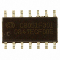
C8051F301-GS Silicon Laboratories Inc, C8051F301-GS Datasheet - Page 126

C8051F301-GS
Manufacturer Part Number
C8051F301-GS
Description
IC 8051 MCU 8K FLASH 14-SOIC
Manufacturer
Silicon Laboratories Inc
Series
C8051F30xr
Specifications of C8051F301-GS
Program Memory Type
FLASH
Program Memory Size
8KB (8K x 8)
Package / Case
14-SOIC (3.9mm Width), 14-SOL
Core Processor
8051
Core Size
8-Bit
Speed
25MHz
Connectivity
SMBus (2-Wire/I²C), UART/USART
Peripherals
POR, PWM, WDT
Number Of I /o
8
Ram Size
256 x 8
Voltage - Supply (vcc/vdd)
2.7 V ~ 3.6 V
Oscillator Type
Internal
Operating Temperature
-40°C ~ 85°C
Processor Series
C8051F3x
Core
8051
Data Bus Width
8 bit
Data Ram Size
256 B
Interface Type
I2C/SMBus/UART
Maximum Clock Frequency
25 MHz
Number Of Programmable I/os
8
Number Of Timers
3
Maximum Operating Temperature
+ 85 C
Mounting Style
SMD/SMT
3rd Party Development Tools
PK51, CA51, A51, ULINK2
Development Tools By Supplier
C8051F300DK
Minimum Operating Temperature
- 40 C
Package
14SOIC
Device Core
8051
Family Name
C8051F30x
Maximum Speed
25 MHz
Operating Supply Voltage
3.3 V
Lead Free Status / RoHS Status
Lead free / RoHS Compliant
For Use With
770-1006 - ISP 4PORT FOR SILABS C8051F MCU336-1444 - ADAPTER PROGRAM TOOLSTICK F300336-1319 - REFERENCE DESIGN STEPPER MOTOR
Eeprom Size
-
Data Converters
-
Lead Free Status / Rohs Status
Lead free / RoHS Compliant
Other names
336-1536-5
C8051F300/1/2/3/4/5
13.5.4. Slave Transmitter Mode
Serial data is transmitted on SDA and the clock is received on SCL. When slave events are enabled (INH
= 0), the interface enters Slave Receiver Mode (to receive the slave address) when a START followed by a
slave address and direction bit (READ in this case) is received. Software responds to the received slave
address with an ACK, or ignores the received slave address with a NACK. If the received address is
ignored, slave interrupts will be inhibited until the next START is detected. If the received slave address is
acknowledged, software should write data to SMB0DAT to force the SMBus into Slave Transmitter Mode.
The switch from Slave Receiver to Slave Transmitter requires software management. Software should per-
form the steps outlined below only when a valid slave address is received (indicated by the label “RX-to-TX
Steps” in Figure 13.8).
The interface enters Slave Transmitter Mode and transmits one or more bytes of data (the above steps are
only required before the first byte of the transfer). After each byte is transmitted, the master sends an
acknowledge bit; if the acknowledge bit is an ACK, SMB0DAT should be written with the next data byte. If
the acknowledge bit is a NACK, SMB0DAT should not be written to before SI is cleared (Note: an error
condition may be generated if SMB0DAT is written following a received NACK while in Slave Transmitter
Mode). The interface exits Slave Transmitter Mode after receiving a STOP. Note that the interface will
switch to Slave Receiver Mode if SMB0DAT is not written following a Slave Transmitter interrupt.
Figure 13.8 shows a typical Slave Transmitter sequence. Two transmitted data bytes are shown, though
any number of bytes may be transmitted. Notice that the ‘data byte transferred’ interrupts occur after the
ACK cycle in this mode.
126
Step 1. Set ACK to ‘1’.
Step 2. Write outgoing data to SMB0DAT.
Step 3. Check SMB0DAT.7; if ‘1’, do not perform steps 4, 6 or 7.
Step 4. Set STO to ‘1’.
Step 5. Clear SI to ‘0’.
Step 6. Poll for TXMODE => ‘1’.
Step 7. Clear STO to ‘0’ (must be done before the next ACK cycle).
S
Received by SMBus
Interface
Transmitted by
SMBus Interface
SLA
Figure 13.8. Typical Slave Transmitter Sequence
Interrupt
Perform RX-to-TX
Steps Here
R
A
Data Byte
Rev. 2.9
Interrupt
A
S = START
P = STOP
N = NACK
W = WRITE
SLA = Slave Address
Data Byte
Interrupt
N
Interrupt
P


