C8051F305-GM Silicon Laboratories Inc, C8051F305-GM Datasheet - Page 9
C8051F305-GM
Manufacturer Part Number
C8051F305-GM
Description
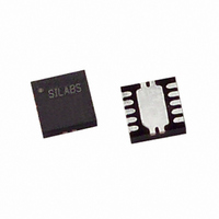
IC 8051 MCU 2K FLASH 11QFN
Manufacturer
Silicon Laboratories Inc
Series
C8051F30xr
Specifications of C8051F305-GM
Program Memory Type
FLASH
Program Memory Size
2KB (2K x 8)
Package / Case
11-VQFN
Core Processor
8051
Core Size
8-Bit
Speed
25MHz
Connectivity
SMBus (2-Wire/I²C), UART/USART
Peripherals
POR, PWM, WDT
Number Of I /o
8
Ram Size
256 x 8
Voltage - Supply (vcc/vdd)
2.7 V ~ 3.6 V
Oscillator Type
External
Operating Temperature
-40°C ~ 85°C
Processor Series
C8051F3x
Core
8051
Data Bus Width
8 bit
Data Ram Size
256 B
Interface Type
I2C/SMBus/UART
Maximum Clock Frequency
25 MHz
Number Of Programmable I/os
8
Number Of Timers
3
Operating Supply Voltage
2.7 V to 3.6 V
Maximum Operating Temperature
+ 85 C
Mounting Style
SMD/SMT
3rd Party Development Tools
PK51, CA51, A51, ULINK2
Development Tools By Supplier
C8051F300DK
Minimum Operating Temperature
- 40 C
On-chip Adc
8 bit, 8 Channel
No. Of I/o's
8
Ram Memory Size
256Byte
Cpu Speed
25MHz
No. Of Timers
3
Rohs Compliant
Yes
Package
11QFN EP
Device Core
8051
Family Name
C8051F30x
Maximum Speed
25 MHz
Lead Free Status / RoHS Status
Lead free / RoHS Compliant
For Use With
770-1006 - ISP 4PORT FOR SILABS C8051F MCU336-1444 - ADAPTER PROGRAM TOOLSTICK F300
Eeprom Size
-
Data Converters
-
Lead Free Status / Rohs Status
Lead free / RoHS Compliant
Other names
336-1251
Available stocks
Company
Part Number
Manufacturer
Quantity
Price
Company:

Part Number:
C8051F305-GM
Manufacturer:
SiliconL
Quantity:
162
Part Number:
C8051F305-GMR
Manufacturer:
SILICONLABS/芯科
Quantity:
20 000


List of Tables
1. System Overview
2. Absolute Maximum Ratings
3. Global Electrical Characteristics
4. Pinout and Package Definitions
5. ADC0 (8-Bit ADC, C8051F300/2)
6. Voltage Reference (C8051F300/2)
7. Comparator0
8. CIP-51 Microcontroller
9. Reset Sources
10. Flash Memory
11. Oscillators
12. Port Input/Output
13. SMBus
14. UART0
Table 1.1. Product Selection Guide ......................................................................... 14
Table 2.1. Absolute Maximum Ratings .................................................................... 24
Table 3.1. Global Electrical Characteristics ............................................................. 25
Table 4.1. Pin Definitions for the C8051F300/1/2/3/4/5 ........................................... 27
Table 4.2. QFN-11 Package Dimensions ................................................................ 29
Table 4.3. QFN-11 Landing Diagram Dimensions ................................................... 31
Table 4.4. SOIC-14 Package Dimensions ............................................................... 33
Table 4.5. SOIC-14 PCB Land Pattern Dimensions ................................................ 34
Table 5.1. ADC0 Electrical Characteristics .............................................................. 47
Table 6.1. External Voltage Reference Circuit Electrical Characteristics ................ 50
Table 7.1. Comparator0 Electrical Characteristics .................................................. 55
Table 8.1. CIP-51 Instruction Set Summary ............................................................ 59
Table 8.2. Special Function Register (SFR) Memory Map ...................................... 66
Table 8.3. Special Function Registers ..................................................................... 66
Table 8.4. Interrupt Summary .................................................................................. 74
Table 9.1. User Code Space Address Limits ........................................................... 86
Table 9.2. Reset Electrical Characteristics .............................................................. 86
Table 10.1. Flash Electrical Characteristics ............................................................ 90
Table 10.2. Security Byte Decoding ........................................................................ 91
Table 11.1. Internal Oscillator Electrical Characteristics ......................................... 99
Table 12.1. Port I/O DC Electrical Characteristics ................................................. 110
Table 13.1. SMBus Clock Source Selection .......................................................... 116
Table 13.2. Minimum SDA Setup and Hold Times ................................................ 117
Table 13.3. Sources for Hardware Changes to SMB0CN ..................................... 121
Table 13.4. SMBus Status Decoding ..................................................................... 127
Table 14.1. Timer Settings for Standard Baud Rates
Table 14.2. Timer Settings for Standard Baud Rates
Using The Internal 24.5 MHz Oscillator .............................................. 138
Using an External 25 MHz Oscillator .................................................. 138
Rev. 2.9
C8051F300/1/2/3/4/5
9
Related parts for C8051F305-GM
Image
Part Number
Description
Manufacturer
Datasheet
Request
R

Part Number:
Description:
SMD/C°/SINGLE-ENDED OUTPUT SILICON OSCILLATOR
Manufacturer:
Silicon Laboratories Inc
Part Number:
Description:
Manufacturer:
Silicon Laboratories Inc
Datasheet:
Part Number:
Description:
N/A N/A/SI4010 AES KEYFOB DEMO WITH LCD RX
Manufacturer:
Silicon Laboratories Inc
Datasheet:
Part Number:
Description:
N/A N/A/SI4010 SIMPLIFIED KEY FOB DEMO WITH LED RX
Manufacturer:
Silicon Laboratories Inc
Datasheet:
Part Number:
Description:
N/A/-40 TO 85 OC/EZLINK MODULE; F930/4432 HIGH BAND (REV E/B1)
Manufacturer:
Silicon Laboratories Inc
Part Number:
Description:
EZLink Module; F930/4432 Low Band (rev e/B1)
Manufacturer:
Silicon Laboratories Inc
Part Number:
Description:
I°/4460 10 DBM RADIO TEST CARD 434 MHZ
Manufacturer:
Silicon Laboratories Inc
Part Number:
Description:
I°/4461 14 DBM RADIO TEST CARD 868 MHZ
Manufacturer:
Silicon Laboratories Inc
Part Number:
Description:
I°/4463 20 DBM RFSWITCH RADIO TEST CARD 460 MHZ
Manufacturer:
Silicon Laboratories Inc
Part Number:
Description:
I°/4463 20 DBM RADIO TEST CARD 868 MHZ
Manufacturer:
Silicon Laboratories Inc
Part Number:
Description:
I°/4463 27 DBM RADIO TEST CARD 868 MHZ
Manufacturer:
Silicon Laboratories Inc
Part Number:
Description:
I°/4463 SKYWORKS 30 DBM RADIO TEST CARD 915 MHZ
Manufacturer:
Silicon Laboratories Inc
Part Number:
Description:
N/A N/A/-40 TO 85 OC/4463 RFMD 30 DBM RADIO TEST CARD 915 MHZ
Manufacturer:
Silicon Laboratories Inc
Part Number:
Description:
I°/4463 20 DBM RADIO TEST CARD 169 MHZ
Manufacturer:
Silicon Laboratories Inc