C8051F305-GM Silicon Laboratories Inc, C8051F305-GM Datasheet - Page 176
C8051F305-GM
Manufacturer Part Number
C8051F305-GM
Description
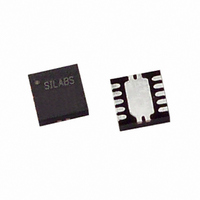
IC 8051 MCU 2K FLASH 11QFN
Manufacturer
Silicon Laboratories Inc
Series
C8051F30xr
Specifications of C8051F305-GM
Program Memory Type
FLASH
Program Memory Size
2KB (2K x 8)
Package / Case
11-VQFN
Core Processor
8051
Core Size
8-Bit
Speed
25MHz
Connectivity
SMBus (2-Wire/I²C), UART/USART
Peripherals
POR, PWM, WDT
Number Of I /o
8
Ram Size
256 x 8
Voltage - Supply (vcc/vdd)
2.7 V ~ 3.6 V
Oscillator Type
External
Operating Temperature
-40°C ~ 85°C
Processor Series
C8051F3x
Core
8051
Data Bus Width
8 bit
Data Ram Size
256 B
Interface Type
I2C/SMBus/UART
Maximum Clock Frequency
25 MHz
Number Of Programmable I/os
8
Number Of Timers
3
Operating Supply Voltage
2.7 V to 3.6 V
Maximum Operating Temperature
+ 85 C
Mounting Style
SMD/SMT
3rd Party Development Tools
PK51, CA51, A51, ULINK2
Development Tools By Supplier
C8051F300DK
Minimum Operating Temperature
- 40 C
On-chip Adc
8 bit, 8 Channel
No. Of I/o's
8
Ram Memory Size
256Byte
Cpu Speed
25MHz
No. Of Timers
3
Rohs Compliant
Yes
Package
11QFN EP
Device Core
8051
Family Name
C8051F30x
Maximum Speed
25 MHz
Lead Free Status / RoHS Status
Lead free / RoHS Compliant
For Use With
770-1006 - ISP 4PORT FOR SILABS C8051F MCU336-1444 - ADAPTER PROGRAM TOOLSTICK F300
Eeprom Size
-
Data Converters
-
Lead Free Status / Rohs Status
Lead free / RoHS Compliant
Other names
336-1251
Available stocks
Company
Part Number
Manufacturer
Quantity
Price
Company:

Part Number:
C8051F305-GM
Manufacturer:
SiliconL
Quantity:
162
Part Number:
C8051F305-GMR
Manufacturer:
SILICONLABS/芯科
Quantity:
20 000


C8051F300/1/2/3/4/5
D
Revision 2.3 to Revision 2.4
•
•
•
•
•
•
•
•
•
•
•
•
•
•
•
•
•
Revision 2.4 to Revision 2.5
•
176
OCUMENT
Removed preliminary tag.
Changed all references of MLP package to
QFN package.
Pinout chapter: Figure 4.3: Changed title to
“Typical QFN-11 Solder Paste Mask.”
ADC chapter: Added reference to minimum
tracking time in the Tracking Modes section.
Comparators chapter: SFR Definition 7.3,
CPT0MD: Updated the register reset value and
the CP0 response time table.
CIP51 chapter: Updated IDLE mode and rec-
ommendations.
CIP51 chapter: Updated Interrupt behavior and
EA recommendations.
CIP51 chapter: SFR Definition 8.4, PSW: Clari-
fied OV flag description.
CIP51 chapter: SFR Definition 8.8, IP register:
Changed “default priority order” to “low priority”
for low priority descriptions.
Reset Sources chapter: Clarified description of
VDD Ramp Time.
Reset Sources chapter: Table 9.2, “Reset Elec-
trical Characteristics”: Added VDD Ramp Time
and changed “VDD POR Threshold” to “VDD
Monitor Threshold.”
FLASH Memory chapter: Clarified descriptions
of FLASH security features.
Oscillators chapter: Table 11.1 “Internal Oscil-
lator Electrical Characteristics”: Added Cali-
brated Internal Oscillator specification over a
smaller temperature range.
Oscillators chapter: Clarified external crystal
initialization steps and added a specific
32.768 kHz crystal example.
Oscillators chapter: Clarified external capacitor
example.
SMBus chapter: Figure 14.5, SMB0CF regis-
ter: Added a description of the behavior of
Timer 3 in split mode if SMBTOE is set.
Timers chapter: Changed references to “TL2”
and “TH2” to “TMR2L” and “TMR2H,” respec-
tively.
Fixed variables and applied formatting
changes.
C
HANGE
L
IST
Rev. 2.9
Revision 2.5 to Revision 2.6
•
Revision 2.6 to Revision 2.7
•
•
•
•
•
Revision 2.7 to Revision 2.8
•
Revision 2.8 to Revision 2.9
•
•
•
•
•
•
•
Updated Table 1.1 Product Selection Guide to
include Lead-free information.
Removed non-RoHS compliant devices from
Table 1.1, “Product Selection Guide,” on
page 14.
Added MIN and MAX specifications for ADC
Offset Error and ADC Full Scale Error to
Table 5.1, “ADC0 Electrical Characteristics,”
on page 47.
Improved power supply specifications in
Table 3.1, “Global Electrical Characteristics,”
on page 25.
Added
Guidelines” on page
Fixed minor typographical errors throughout.
Updated block diagram on page 1.
Updated QFN package drawings and notes.
Added SOIC-14 package information.
Added text to CPT0CN's SFR definition to indi-
cate that the SFR is bit addressable.
Changed SMBus maximum transfer speed
from 1/10th system clock to 1/20th system
clock in SMBus section.
Added information pertaining to Slave
Receiver and Slave Transmitter states in Table
13.4.
Changed Table 5.1 and Figure 5.4 to indicate
that 11 SAR clocks are needed for a SAR con-
version to complete.
Changed SCON0s SFR definition to show that
SCON0 bit 6 always resets to a value of 1.
Section “10.4. Flash Write and Erase
94.
Related parts for C8051F305-GM
Image
Part Number
Description
Manufacturer
Datasheet
Request
R

Part Number:
Description:
SMD/C°/SINGLE-ENDED OUTPUT SILICON OSCILLATOR
Manufacturer:
Silicon Laboratories Inc
Part Number:
Description:
Manufacturer:
Silicon Laboratories Inc
Datasheet:
Part Number:
Description:
N/A N/A/SI4010 AES KEYFOB DEMO WITH LCD RX
Manufacturer:
Silicon Laboratories Inc
Datasheet:
Part Number:
Description:
N/A N/A/SI4010 SIMPLIFIED KEY FOB DEMO WITH LED RX
Manufacturer:
Silicon Laboratories Inc
Datasheet:
Part Number:
Description:
N/A/-40 TO 85 OC/EZLINK MODULE; F930/4432 HIGH BAND (REV E/B1)
Manufacturer:
Silicon Laboratories Inc
Part Number:
Description:
EZLink Module; F930/4432 Low Band (rev e/B1)
Manufacturer:
Silicon Laboratories Inc
Part Number:
Description:
I°/4460 10 DBM RADIO TEST CARD 434 MHZ
Manufacturer:
Silicon Laboratories Inc
Part Number:
Description:
I°/4461 14 DBM RADIO TEST CARD 868 MHZ
Manufacturer:
Silicon Laboratories Inc
Part Number:
Description:
I°/4463 20 DBM RFSWITCH RADIO TEST CARD 460 MHZ
Manufacturer:
Silicon Laboratories Inc
Part Number:
Description:
I°/4463 20 DBM RADIO TEST CARD 868 MHZ
Manufacturer:
Silicon Laboratories Inc
Part Number:
Description:
I°/4463 27 DBM RADIO TEST CARD 868 MHZ
Manufacturer:
Silicon Laboratories Inc
Part Number:
Description:
I°/4463 SKYWORKS 30 DBM RADIO TEST CARD 915 MHZ
Manufacturer:
Silicon Laboratories Inc
Part Number:
Description:
N/A N/A/-40 TO 85 OC/4463 RFMD 30 DBM RADIO TEST CARD 915 MHZ
Manufacturer:
Silicon Laboratories Inc
Part Number:
Description:
I°/4463 20 DBM RADIO TEST CARD 169 MHZ
Manufacturer:
Silicon Laboratories Inc