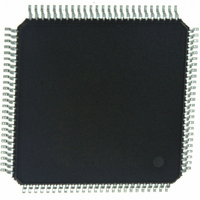
Z16F2811AL20SG Zilog, Z16F2811AL20SG Datasheet - Page 333

Z16F2811AL20SG
Manufacturer Part Number
Z16F2811AL20SG
Description
IC ZNEO MCU FLASH 128K 100LQFP
Manufacturer
Zilog
Series
Encore!® ZNEOr
Specifications of Z16F2811AL20SG
Core Processor
ZNEO
Core Size
16-Bit
Speed
20MHz
Connectivity
EBI/EMI, I²C, IrDA, LIN, SPI, UART/USART
Peripherals
Brown-out Detect/Reset, DMA, POR, PWM, WDT
Number Of I /o
76
Program Memory Size
128KB (128K x 8)
Program Memory Type
FLASH
Ram Size
4K x 8
Voltage - Supply (vcc/vdd)
2.7 V ~ 3.6 V
Data Converters
A/D 12x10b
Oscillator Type
Internal
Operating Temperature
0°C ~ 70°C
Package / Case
100-LQFP
Processor Series
Z16F2x
Core
Zneo
Data Bus Width
16 bit
Data Ram Size
4 B
Interface Type
ESPI, I2C, UART
Maximum Clock Frequency
20 MHz
Number Of Programmable I/os
76
Number Of Timers
4
Operating Supply Voltage
2.7 V to 3.6 V
Maximum Operating Temperature
+ 70 C
Mounting Style
SMD/SMT
Development Tools By Supplier
Z16F2800100ZCOG
Minimum Operating Temperature
0 C
On-chip Adc
10 bit, 12 Channel
For Use With
770-1003 - ISP 4PORT FOR ZILOG ZNEO MCU269-4537 - DEV KIT FOR Z16F ZNEO
Lead Free Status / RoHS Status
Lead free / RoHS Compliant
Eeprom Size
-
Lead Free Status / Rohs Status
Details
Other names
269-4533
Available stocks
Company
Part Number
Manufacturer
Quantity
Price
Company:
Part Number:
Z16F2811AL20SG
Manufacturer:
VISHAY
Quantity:
9 487
Part Number:
Z16F2811AL20SG
Manufacturer:
ZILOG
Quantity:
20 000
- Current page: 333 of 388
- Download datasheet (22Mb)
Table 170. Line Control Register (DBGLCR)
PS022008-0810
Table 169. Baud Rate Reload Register (DBGBR)
BITS
FIELD
RESET
R/W
ADDR
BITS
FIELD
RESET
R/W
ADDR
Baud Rate Reload Register
Line Control Register
15
R/W
OE
The
communication stream. This register is automatically set by the Auto-Baud Detector. This
register cannot be written by the CPU when
RELOAD—This value is the baud rate reload value used to generate a bit clock. It is
calculated as
The
cannot be written by the CPU when
OE—Output enable
This bit controls the output driver. If the UART is enabled, this bit controls the output
driver during transmission only.
0 = Pin is open-drain during UART transmit. Pin behaves as an input if UART is disabled.
1 = Pin is driven during transmission if UART is enabled. Pin is an output if UART is
disabled.
7
0
14
Baud Rate Reload Register (DBGBR)
Line Control Register (DBGLCR)
13
TDH
R/W
6
0
12
RELOAD = SYSTEM CLOCK
11
HDS
R/W
5
0
10
P R E L I M I N A R Y
FF_E082-FF_E083
9
BAUD RATE
TXFC
R/W
4
OCDLOCK
0
RELOAD
FF_E084
8
0000H
controls the state of the UART. This register
R/W
is used to configure the baud rate of the serial
OCDLOCK
7
NBEN
is set.
R/W
3
0
6
x 8
is set.
5
R/W
NB
2
0
4
Product Specification
ZNEO
3
OUT
R/W
On-Chip Debugger
1
1
2
Z16F Series
1
PIN
X
R
0
0
317
Related parts for Z16F2811AL20SG
Image
Part Number
Description
Manufacturer
Datasheet
Request
R

Part Number:
Description:
High Performance Microcontrollers
Manufacturer:
ZiLOG Semiconductor
Datasheet:

Part Number:
Description:
Communication Controllers, ZILOG INTELLIGENT PERIPHERAL CONTROLLER (ZIP)
Manufacturer:
Zilog, Inc.
Datasheet:

Part Number:
Description:
KIT DEV FOR Z8 ENCORE 16K TO 64K
Manufacturer:
Zilog
Datasheet:

Part Number:
Description:
KIT DEV Z8 ENCORE XP 28-PIN
Manufacturer:
Zilog
Datasheet:

Part Number:
Description:
DEV KIT FOR Z8 ENCORE 8K/4K
Manufacturer:
Zilog
Datasheet:

Part Number:
Description:
KIT DEV Z8 ENCORE XP 28-PIN
Manufacturer:
Zilog
Datasheet:

Part Number:
Description:
DEV KIT FOR Z8 ENCORE 4K TO 8K
Manufacturer:
Zilog
Datasheet:

Part Number:
Description:
CMOS Z8 microcontroller. ROM 16 Kbytes, RAM 256 bytes, speed 16 MHz, 32 lines I/O, 3.0V to 5.5V
Manufacturer:
Zilog, Inc.
Datasheet:

Part Number:
Description:
Low-cost microcontroller. 512 bytes ROM, 61 bytes RAM, 8 MHz
Manufacturer:
Zilog, Inc.
Datasheet:

Part Number:
Description:
Z8 4K OTP Microcontroller
Manufacturer:
Zilog, Inc.
Datasheet:

Part Number:
Description:
CMOS SUPER8 ROMLESS MCU
Manufacturer:
Zilog, Inc.
Datasheet:

Part Number:
Description:
SL1866 CMOSZ8 OTP Microcontroller
Manufacturer:
Zilog, Inc.
Datasheet:

Part Number:
Description:
SL1866 CMOSZ8 OTP Microcontroller
Manufacturer:
Zilog, Inc.
Datasheet:

Part Number:
Description:
OTP (KB) = 1, RAM = 125, Speed = 12, I/O = 14, 8-bit Timers = 2, Comm Interfaces Other Features = Por, LV Protect, Voltage = 4.5-5.5V
Manufacturer:
Zilog, Inc.
Datasheet:


