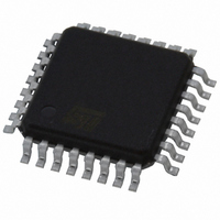
ST72F324BK4T3 STMicroelectronics, ST72F324BK4T3 Datasheet - Page 32

ST72F324BK4T3
Manufacturer Part Number
ST72F324BK4T3
Description
IC MCU 8BIT 16K FLASH 32-TQFP
Manufacturer
STMicroelectronics
Series
ST7r
Datasheet
1.ST72F324BJ2T6.pdf
(198 pages)
Specifications of ST72F324BK4T3
Core Processor
ST7
Core Size
8-Bit
Speed
8MHz
Connectivity
SCI, SPI
Peripherals
LVD, POR, PWM, WDT
Number Of I /o
24
Program Memory Size
16KB (16K x 8)
Program Memory Type
FLASH
Ram Size
512 x 8
Voltage - Supply (vcc/vdd)
3.8 V ~ 5.5 V
Data Converters
A/D 12x10b
Oscillator Type
Internal
Operating Temperature
-40°C ~ 125°C
Package / Case
32-TQFP, 32-VQFP
Processor Series
ST72F3x
Core
ST7
Data Bus Width
8 bit
Data Ram Size
512 B
Interface Type
SCI, SPI
Maximum Clock Frequency
8 MHz
Number Of Programmable I/os
32
Number Of Timers
3
Maximum Operating Temperature
+ 125 C
Mounting Style
SMD/SMT
Development Tools By Supplier
ST7232X-EVAL, ST7MDT20-DVP3, ST7MDT20J-EMU3, STX-RLINK
Minimum Operating Temperature
- 40 C
On-chip Adc
10 bit, 12 Channel
A/d Bit Size
10 bit
A/d Channels Available
12
Height
1.4 mm
Length
7 mm
Supply Voltage (max)
5.5 V
Supply Voltage (min)
3.8 V
Width
7 mm
For Use With
497-6421 - BOARD EVAL DGTL BATT CHGR DESIGN497-5046 - KIT TOOL FOR ST7/UPSD/STR7 MCU
Lead Free Status / RoHS Status
Lead free / RoHS Compliant
Eeprom Size
-
Lead Free Status / Rohs Status
Details
Other names
497-8241
ST72F324BK4T3
ST72F324BK4T3
Available stocks
Company
Part Number
Manufacturer
Quantity
Price
Company:
Part Number:
ST72F324BK4T3
Manufacturer:
STMicroelectronics
Quantity:
10 000
Company:
Part Number:
ST72F324BK4T3TR
Manufacturer:
STMicroelectronics
Quantity:
10 000
Supply, reset and clock management
Figure 10. Clock, reset and supply block diagram
6.3
Caution:
6.3.1
32/198
RESET
OSC2
OSC1
V
V
DD
SS
Multi-oscillator (MO)
The main clock of the ST7 can be generated by three different source types coming from the
multi-oscillator block:
●
●
●
Each oscillator is optimized for a given frequency range in terms of consumption and is
selectable through the option byte. The associated hardware configurations are shown in
Table
The OSC1 and/or OSC2 pins must not be left unconnected. For the purposes of Failure
Mode and Effect Analysis, it should be noted that if the OSC1 and/or OSC2 pins are left
unconnected, the ST7 main oscillator may start and, in this configuration, could generate an
f
unsafe/undefined state. The product behavior must therefore be considered undefined when
the OSC pins are left unconnected.
External clock source
In this external clock mode, a clock signal (square, sinus or triangle) with ~50% duty cycle
has to drive the OSC1 pin while the OSC2 pin is tied to ground.
OSC
an external source
4 crystal or ceramic resonator oscillators
an internal high frequency RC oscillator
clock frequency in excess of the allowed maximum (> 16 MHz.), putting the ST7 in an
9. Refer to the electrical characteristics section for more details.
Reset Sequence
Oscillator
Multi-
(MO)
Manager
(RSM)
f
OSC
(option)
PLL
Doc ID13466 Rev 4
SICSR
0
System Integrity Management
AVD AVD LVD
IE
AVD Interrupt Request
F
Auxiliary Voltage
Low Voltage
RF
Detector
Detector
(AVD)
(LVD)
0
0
0
WDG
f
RF
OSC2
Clock (MCC/RTC)
with Real-time
timer (WDG)
Main Clock
Watchdog
Controller
ST72324B-Auto
f
CPU


