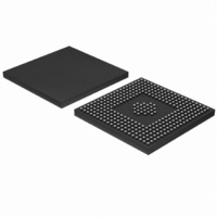
LH7A404N0F000B3;55 NXP Semiconductors, LH7A404N0F000B3;55 Datasheet - Page 42

LH7A404N0F000B3;55
Manufacturer Part Number
LH7A404N0F000B3;55
Description
IC ARM9 BLUESTREAK MCU 324LFBGA
Manufacturer
NXP Semiconductors
Series
BlueStreak ; LH7Ar
Datasheet
1.LH7A404N0F000B355.pdf
(75 pages)
Specifications of LH7A404N0F000B3;55
Package / Case
324-LFBGA
Core Processor
ARM9
Core Size
16/32-Bit
Speed
200MHz
Connectivity
EBI/EMI, IrDA, Microwire, MMC, PS2, SmartCard, SPI, SSI, SSP, UART/USART, USB
Peripherals
AC'97, DMA, LCD, POR, PWM, WDT
Number Of I /o
64
Program Memory Type
ROMless
Ram Size
80K x 8
Voltage - Supply (vcc/vdd)
1.71 V ~ 3.6 V
Data Converters
A/D 9x10b
Oscillator Type
External
Operating Temperature
-40°C ~ 85°C
Processor Series
LH7A4
Core
ARM9TDMI
Data Bus Width
32 bit
Data Ram Size
80 KB
Interface Type
JTAG, SPI, UART
Maximum Clock Frequency
200 MHz
Number Of Programmable I/os
64
Number Of Timers
3
Operating Supply Voltage
1.8 V
Maximum Operating Temperature
+ 85 C
Mounting Style
SMD/SMT
3rd Party Development Tools
MDK-ARM, RL-ARM, ULINK2
Minimum Operating Temperature
- 40 C
On-chip Adc
10 bit, 9 Channel
Lead Free Status / RoHS Status
Lead free / RoHS Compliant
For Use With
568-4304 - BOARD EVAL FOR LH7A404
Eeprom Size
-
Program Memory Size
-
Lead Free Status / Rohs Status
Lead free / RoHS Compliant
Other names
568-4335
935285069557
LH7A404N0F000B3
935285069557
LH7A404N0F000B3
LH7A404
TIMING FOR nWAIT SIGNALLING
Wait States, the SMC also can use nWAIT signalling to
extend transactions. When the nWAIT input is asserted,
the current transaction is held in suspense until nWAIT
NOTES:
1. The timing relationship is specified as a cycle-based timing.
2. The Bank Configuration Register (BCRx:WST1) must have Read
3. The number of HCLK periods that nWAIT lags assertion of nCSx
42
tDA_nCS(x)_nWAIT
tDD_nWAIT_nCS(x)
tDD_nWAIT_nOE
tA_nWAIT
NOTES:
SQ: nWAIT Sampled and Queued
SI: nWAIT Sampled and Ignored
In addition to being able to program the number of
Variations caused by clock jitter, power rail noise, and I/O cond-
tioning will cause these timings to vary nominally. It is recom-
mended that designers add a small margin to avoid possible
corner-case conditions.
Wait States set to a minimum of 2.
must be added to the minimum value for BCRx:WST1. For exam-
ple, if nWAIT lags nCSx by 3 HCLK periods, the minimum setting
of BCRx:WST1 is 2 + 3, or a total of 5 as the minimum value for
BCRx:WST1.
nCS(x)
nWAIT
HCLK
Transaction
Sequence
nOE
PARAMETER
Figure 12. nWAIT Read Sequence (BCRx:WST1 = 2); Minimum Wait State Example
tDA_nCS(x)_nWAIT
WSD-2
DELAY
Delay from nCS(x) assertion to nWAIT assertion
Delay from nWAIT deassertion to nCS(x) deassertion
Delay from nWAIT deassertion to nOE deassertion
Assertion time of nWAIT
SQ-4
WSD-1
DELAY
SQ-3
WSD-0
DELAY
tA_nWAIT
SQ-2
DELAY
nWAIT
SQ-4
DESCRIPTION
NXP Semiconductors
SQ-1
DELAY
nWAIT
SQ-3
SQ-0
is released, allowing slow memory or memory-mapped
peripherals time to complete the action.
timing using different WST register settings and
circumstances.
4. No nWAIT delay cycles are added for any nWAIT assertions that
5. Once the WSD-2 delay begins, one HCLK cycle is added to the
6. Once nWAIT is sampled HIGH (de-asserted), the current memory
7. Since static and dynamic memory cannot be accessed at the
DELAY
nWAIT
SQ-2
Figure 12 through Figure 17 illustrate nWAIT
occur prior to the beginning of the WSD-2 delay. These nWAIT
assertions are ignored.
transaction each time nWAIT is sampled and queued (SQ-x). The
nWAIT cycles begin being added after the Wait State Countdown
reaches WSD-0.
transaction is queued to complete.
same time, prolonged extension of an SMC transaction by either
Wait States or nWAIT delays can cause refresh failure for the
SDRAM, and may cause SDRAM data loss.
DELAY
nWAIT
tDD_nWAIT_nCS(x)
SQ-1
tDD_nWAIT_nOE
DELAY
nWAIT
SQ-0
MIN.
CYCLE
END
0
2
32-Bit System-on-Chip
Preliminary data sheet
MAX.
29
4
4
HCLK periods
HCLK periods
HCLK periods
HCLK periods
UNIT
LH7A404-203
1


