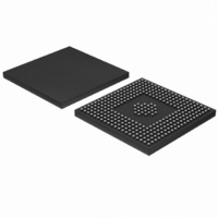
LH7A404N0F000B3;55 NXP Semiconductors, LH7A404N0F000B3;55 Datasheet - Page 28

LH7A404N0F000B3;55
Manufacturer Part Number
LH7A404N0F000B3;55
Description
IC ARM9 BLUESTREAK MCU 324LFBGA
Manufacturer
NXP Semiconductors
Series
BlueStreak ; LH7Ar
Datasheet
1.LH7A404N0F000B355.pdf
(75 pages)
Specifications of LH7A404N0F000B3;55
Package / Case
324-LFBGA
Core Processor
ARM9
Core Size
16/32-Bit
Speed
200MHz
Connectivity
EBI/EMI, IrDA, Microwire, MMC, PS2, SmartCard, SPI, SSI, SSP, UART/USART, USB
Peripherals
AC'97, DMA, LCD, POR, PWM, WDT
Number Of I /o
64
Program Memory Type
ROMless
Ram Size
80K x 8
Voltage - Supply (vcc/vdd)
1.71 V ~ 3.6 V
Data Converters
A/D 9x10b
Oscillator Type
External
Operating Temperature
-40°C ~ 85°C
Processor Series
LH7A4
Core
ARM9TDMI
Data Bus Width
32 bit
Data Ram Size
80 KB
Interface Type
JTAG, SPI, UART
Maximum Clock Frequency
200 MHz
Number Of Programmable I/os
64
Number Of Timers
3
Operating Supply Voltage
1.8 V
Maximum Operating Temperature
+ 85 C
Mounting Style
SMD/SMT
3rd Party Development Tools
MDK-ARM, RL-ARM, ULINK2
Minimum Operating Temperature
- 40 C
On-chip Adc
10 bit, 9 Channel
Lead Free Status / RoHS Status
Lead free / RoHS Compliant
For Use With
568-4304 - BOARD EVAL FOR LH7A404
Eeprom Size
-
Program Memory Size
-
Lead Free Status / Rohs Status
Lead free / RoHS Compliant
Other names
568-4335
935285069557
LH7A404N0F000B3
935285069557
LH7A404N0F000B3
LH7A404
• Battery voltage sense in addition to normal direct
• A 9-channel multiplexer for routing user-selected
• A 16 × 16 FIFO for 10-bit digital output of A/D
• A pen-down sensor to generate interrupts to the host
• Low-power circuitry and power control modes to
• Conversion automation for flexibility while minimizing
• A brownout detector with separate interrupt
Battery Monitor Interface (BMI)
fied for two types of battery monitors/gas gauges. The
first type employs a single wire interface. The second
interface employs a two-wire multi-master bus, imple-
menting the Smart Battery System Specification.
If both interfaces are enabled at the same time, the
Single Wire Interface has priority.
SINGLE WIRE INTERFACE
• Serial-to-parallel conversion on data received from
• Parallel-to-serial conversion on data transmitted to
• Data packet coding/decoding on data transfers
protocol in which the host initiates a data transfer by
sending a WriteData/Command word to the battery
monitor.
SMART BATTERY INTERFACE
• Serial-to-parallel conversion on data received from
• Parallel-to-serial conversion of data transmitted to
master bus (the SMBus), allowing multiple bus masters
to be connected to it. A master device initiates a bus
transfer and provides the clock signals. A slave device
can receive data provided by the master or it can pro-
vide data to the master. Since more than one device
may attempt to take control of the bus as a master,
SMBus provides an arbitration mechanism by relying
on the wired-AND connection of all SMBus interfaces
to the SMBus.
28
voltage inputs
inputs to A/D
minimize on-chip power dissipation
CPU management and interrupt overhead
the peripheral device
the peripheral device
(incorporating Start/Data/Stop data packets)
the peripheral device
the peripheral device.
The BMI is a serial communication interface speci-
The Single Wire Interface performs:
The Single Wire interface uses a command-based
The Smart Battery Interface performs:
The Smart Battery Interface uses a two-wire multi-
NXP Semiconductors
DC-to-DC Converter
• Dual-drive PWM outputs with independent closed
• Software programmable configuration of one of 8
• Software programmable configuration of duty cycle
• Hardware-configured output polarity (for positive or
• Dynamically switched PWM outputs to one of a pair
Watchdog Timer (WDT)
against malfunctions. It is a programmable timer that is
reset by software at regular intervals. Failure to reset
the timer will cause an FIQ interrupt. Failure to service
the FIQ interrupt generates a system reset.
• Timing derived from the system clock
• 16 programmable time-out periods: 2
• Generates a system reset (resets LH7A404) or a
• Software enable, lockout, and counter-reset mecha-
• Protection mechanism guards against interrupt-
General Purpose I/O (GPIO)
and a data direction register. It also has added regis-
ters including Keyboard Scan, PINMUX, GPIO Inter-
rupt Enable, INTYPE1/2, GPIOFEOI and PGHCON.
port is configured as an input or an output while the
data register is used to read the value of the GPIO pins.
GPIOFEOI registers control edge-triggered Interrupts
on Port F. The PINMUX register controls which signals
are from Port D and Port E when they are set as out-
puts, while the PGHCON controls the operations of
Port G and Port H.
loop feedback
output frequencies (each being a fixed division of the
input clock).
from 0 to 15/16, in intervals of 1/16.
negative voltage generation) during power-on reset
via the polarity select inputs
of preprogrammed frequency/duty cycle combina-
tions via external pins.
clock cycles
FIQ interrupt whenever a time-out period is reached
nisms add security against inadvertent writes
The features of the DC-DC Converter interface are:
The Watchdog Timer provides hardware protection
Features of the WDT:
– The first WDT time-out triggers FIQ and asserts
– If FIQ service routine fails to clear nWDFIQ, then
The GPIO has eight ports, each with a data register
The data direction register determines whether a
The GPIO Interrupt Enable, INTYPE[2:1], and the
service-failure:
nWDFIQ status flag
the next WDT time-out triggers a system reset.
32-Bit System-on-Chip
Preliminary data sheet
16
through 2
31


