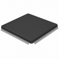
LPC2378FBD144,551 NXP Semiconductors, LPC2378FBD144,551 Datasheet - Page 8

LPC2378FBD144,551
Manufacturer Part Number
LPC2378FBD144,551
Description
IC ARM7 MCU FLASH 512K 144LQFP
Manufacturer
NXP Semiconductors
Series
LPC2300r
Datasheet
1.LPC2377FBD144551.pdf
(68 pages)
Specifications of LPC2378FBD144,551
Program Memory Type
FLASH
Program Memory Size
512KB (512K x 8)
Package / Case
144-LQFP
Core Processor
ARM7
Core Size
16/32-Bit
Speed
72MHz
Connectivity
CAN, EBI/EMI, Ethernet, I²C, Microwire, MMC, SPI, SSI, SSP, UART/USART, USB
Peripherals
Brown-out Detect/Reset, DMA, I²S, POR, PWM, WDT
Number Of I /o
104
Ram Size
58K x 8
Voltage - Supply (vcc/vdd)
3 V ~ 3.6 V
Data Converters
A/D 8x10b; D/A 1x10b
Oscillator Type
Internal
Operating Temperature
-40°C ~ 85°C
Processor Series
LPC23
Core
ARM7TDMI-S
Data Bus Width
16 bit, 32 bit
Data Ram Size
58 KB
Interface Type
CAN/I2S/ISP/UART/USB
Maximum Clock Frequency
72 MHz
Number Of Programmable I/os
104
Number Of Timers
4
Operating Supply Voltage
3.3 V
Maximum Operating Temperature
+ 85 C
Mounting Style
SMD/SMT
3rd Party Development Tools
MDK-ARM, RL-ARM, ULINK2, KSDKLPC2378-02, MCB2370, MCB2370U, MCB2370UME
Development Tools By Supplier
OM10094
Minimum Operating Temperature
- 40 C
On-chip Adc
8-ch x 10-bit
On-chip Dac
1-ch x 10-bit
Lead Free Status / RoHS Status
Lead free / RoHS Compliant
For Use With
568-4310 - EVAL BOARD LPC2158 W/LCDMCB2370UME - BOARD EVAL MCB2370 + ULINK-MEMCB2370U - BOARD EVAL MCB2370 + ULINK2MCB2370 - BOARD EVAL NXP LPC2368/2378568-3999 - BOARD EVAL FOR LPC23 ARM MCU622-1005 - USB IN-CIRCUIT PROG ARM7 LPC2K
Eeprom Size
-
Lead Free Status / Rohs Status
Lead free / RoHS Compliant
Other names
568-3998
935282458551
LPC2378FBD144-S
935282458551
LPC2378FBD144-S
Available stocks
Company
Part Number
Manufacturer
Quantity
Price
Company:
Part Number:
LPC2378FBD144,551
Manufacturer:
ADI
Quantity:
2 397
Company:
Part Number:
LPC2378FBD144,551
Manufacturer:
NXP Semiconductors
Quantity:
10 000
NXP Semiconductors
Table 3.
LPC2377_78
Product data sheet
Symbol
P0[18]/DCD1/
MOSI0/MOSI
P0[19]/DSR1/
MCICLK/SDA1
P0[20]/DTR1/
MCICMD/SCL1
P0[21]/RI1/
MCIPWR/RD1
P0[22]/RTS1/
MCIDAT0/TD1
P0[23]/AD0[0]/
I2SRX_CLK/
CAP3[0]
P0[24]/AD0[1]/
I2SRX_WS/
CAP3[1]
P0[25]/AD0[2]/
I2SRX_SDA/
TXD3
P0[26]/AD0[3]/
AOUT/RXD3
P0[27]/SDA0
Pin description
Pin
86
85
83
82
80
13
11
10
8
35
[2]
[3]
[1]
[1]
[1]
[1]
[1]
[2]
[2]
[4]
…continued
Type
I/O
I
I/O
I/O
I/O
I
O
I/O
I/O
O
I
I/O
I/O
I
O
I
I/O
O
O
O
I/O
I
I/O
I
I/O
I
I/O
I
I/O
I
I/O
O
I/O
I
O
I
I/O
I/O
Description
P0[18] — General purpose digital input/output pin.
DCD1 — Data Carrier Detect input for UART1.
MOSI0 — Master Out Slave In for SSP0.
MOSI — Master Out Slave In for SPI.
P0[19] — General purpose digital input/output pin.
DSR1 — Data Set Ready input for UART1.
MCICLK — Clock output line for SD/MMC interface.
SDA1 — I
P0[20] — General purpose digital input/output pin.
DTR1 — Data Terminal Ready output for UART1.
MCICMD — Command line for SD/MMC interface.
SCL1 — I
P0[21] — General purpose digital input/output pin.
RI1 — Ring Indicator input for UART1.
MCIPWR — Power Supply Enable for external SD/MMC power supply.
RD1 — CAN1 receiver input. (LPC2378 only)
P0[22] — General purpose digital input/output pin.
RTS1 — Request to Send output for UART1.
MCIDAT0 — Data line for SD/MMC interface.
TD1 — CAN1 transmitter output. (LPC2378 only)
P0[23] — General purpose digital input/output pin.
AD0[0] — A/D converter 0, input 0.
I2SRX_CLK — Receive Clock. It is driven by the master and received by the slave.
Corresponds to the signal SCK in the I
CAP3[0] — Capture input for Timer 3, channel 0.
P0[24] — General purpose digital input/output pin.
AD0[1] — A/D converter 0, input 1.
I2SRX_WS — Receive Word Select. It is driven by the master and received by the
slave. Corresponds to the signal WS in the I
CAP3[1] — Capture input for Timer 3, channel 1.
P0[25] — General purpose digital input/output pin.
AD0[2] — A/D converter 0, input 2.
I2SRX_SDA — Receive data. It is driven by the transmitter and read by the
receiver. Corresponds to the signal SD in the I
TXD3 — Transmitter output for UART3.
P0[26] — General purpose digital input/output pin.
AD0[3] — A/D converter 0, input 3.
AOUT — D/A converter output.
RXD3 — Receiver input for UART3.
P0[27] — General purpose digital input/output pin. Output is open-drain.
SDA0 — I
All information provided in this document is subject to legal disclaimers.
2
2
2
C1 clock input/output (this is not an open-drain pin).
C1 data input/output (this is not an open-drain pin).
C0 data input/output. Open-drain output (for I
Rev. 5 — 17 June 2010
Single-chip 16-bit/32-bit microcontrollers
2
S-bus specification.
2
S-bus specification.
2
S-bus specification.
2
LPC2377/78
C-bus compliance).
© NXP B.V. 2010. All rights reserved.
8 of 68


