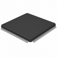
LPC2378FBD144,551 NXP Semiconductors, LPC2378FBD144,551 Datasheet - Page 14

LPC2378FBD144,551
Manufacturer Part Number
LPC2378FBD144,551
Description
IC ARM7 MCU FLASH 512K 144LQFP
Manufacturer
NXP Semiconductors
Series
LPC2300r
Datasheet
1.LPC2377FBD144551.pdf
(68 pages)
Specifications of LPC2378FBD144,551
Program Memory Type
FLASH
Program Memory Size
512KB (512K x 8)
Package / Case
144-LQFP
Core Processor
ARM7
Core Size
16/32-Bit
Speed
72MHz
Connectivity
CAN, EBI/EMI, Ethernet, I²C, Microwire, MMC, SPI, SSI, SSP, UART/USART, USB
Peripherals
Brown-out Detect/Reset, DMA, I²S, POR, PWM, WDT
Number Of I /o
104
Ram Size
58K x 8
Voltage - Supply (vcc/vdd)
3 V ~ 3.6 V
Data Converters
A/D 8x10b; D/A 1x10b
Oscillator Type
Internal
Operating Temperature
-40°C ~ 85°C
Processor Series
LPC23
Core
ARM7TDMI-S
Data Bus Width
16 bit, 32 bit
Data Ram Size
58 KB
Interface Type
CAN/I2S/ISP/UART/USB
Maximum Clock Frequency
72 MHz
Number Of Programmable I/os
104
Number Of Timers
4
Operating Supply Voltage
3.3 V
Maximum Operating Temperature
+ 85 C
Mounting Style
SMD/SMT
3rd Party Development Tools
MDK-ARM, RL-ARM, ULINK2, KSDKLPC2378-02, MCB2370, MCB2370U, MCB2370UME
Development Tools By Supplier
OM10094
Minimum Operating Temperature
- 40 C
On-chip Adc
8-ch x 10-bit
On-chip Dac
1-ch x 10-bit
Lead Free Status / RoHS Status
Lead free / RoHS Compliant
For Use With
568-4310 - EVAL BOARD LPC2158 W/LCDMCB2370UME - BOARD EVAL MCB2370 + ULINK-MEMCB2370U - BOARD EVAL MCB2370 + ULINK2MCB2370 - BOARD EVAL NXP LPC2368/2378568-3999 - BOARD EVAL FOR LPC23 ARM MCU622-1005 - USB IN-CIRCUIT PROG ARM7 LPC2K
Eeprom Size
-
Lead Free Status / Rohs Status
Lead free / RoHS Compliant
Other names
568-3998
935282458551
LPC2378FBD144-S
935282458551
LPC2378FBD144-S
Available stocks
Company
Part Number
Manufacturer
Quantity
Price
Company:
Part Number:
LPC2378FBD144,551
Manufacturer:
ADI
Quantity:
2 397
Company:
Part Number:
LPC2378FBD144,551
Manufacturer:
NXP Semiconductors
Quantity:
10 000
NXP Semiconductors
Table 3.
LPC2377_78
Product data sheet
Symbol
P4[24]/OE
P4[25]/BLS0
P4[28]/MAT2[0]/
TXD3
P4[29]/MAT2[1]/
RXD3
P4[30]/CS0
P4[31]/CS1
ALARM
USB_D−2
DBGEN
TDO
TDI
TMS
TRST
TCK
RTCK
RSTOUT
RESET
XTAL1
XTAL2
RTCX1
RTCX2
V
V
SS
SSA
Pin description
Pin
127
124
118
122
130
134
26
37
6
1
3
4
5
7
143
20
24
31
33
23
25
22, 44,
59, 65,
79, 103,
117,119,
139
15
[1]
[1]
[1]
[1]
[1]
[1]
[8]
[7]
[8][9]
[8][9]
[8][10]
[8][10]
[12]
[1]
[1]
[1]
[1]
[1]
[1]
[1]
[11]
…continued
Type
I/O
O
I/O
O
I/O
O
O
I/O
O
I
I/O
O
I/O
O
O
I/O
I
O
I
I
I
I
I/O
O
I
I
O
I
O
I
I
Description
P4[24] — General purpose digital input/output pin.
OE — LOW active Output Enable signal.
P4[25] — General purpose digital input/output pin.
BLS0 — LOW active Byte Lane select signal 0.
P4 [28] — General purpose digital input/output pin.
MAT2[0] — Match output for Timer 2, channel 0.
TXD3 — Transmitter output for UART3.
P4[29] — General purpose digital input/output pin.
MAT2[1] — Match output for Timer 2, channel 1.
RXD3 — Receiver input for UART3.
P4[30] — General purpose digital input/output pin.
CS0 — LOW active Chip Select 0 signal.
P4[31] — General purpose digital input/output pin.
CS1 — LOW active Chip Select 1 signal.
ALARM — RTC controlled output. This is a 1.8 V pin. It goes HIGH when a RTC
alarm is generated.
USB_D−2 — USB2 port bidirectional D− line. LPC2378 only. This pin is not
connected on the LPC2377.
DBGEN — JTAG interface control signal. Also used for boundary scanning.
TDO — Test Data out for JTAG interface.
TDI — Test Data in for JTAG interface.
TMS — Test Mode Select for JTAG interface.
TRST — Test Reset for JTAG interface.
TCK — Test Clock for JTAG interface. This clock must be slower than
clock (CCLK) for the JTAG interface to operate.
RTCK — JTAG interface control signal.
Note: LOW on this pin while RESET is LOW enables ETM pins (P2[9:0]) to operate
as Trace port after reset.
RSTOUT — This is a 3.3 V pin. LOW on this pin indicates LPC2377/78 being in
Reset state.
external reset input: A LOW on this pin resets the device, causing I/O ports and
peripherals to take on their default states, and processor execution to begin at
address 0. TTL with hysteresis, 5 V tolerant.
Input to the oscillator circuit and internal clock generator circuits.
Output from the oscillator amplifier.
Input to the RTC oscillator circuit.
Output from the RTC oscillator circuit.
ground: 0 V reference.
analog ground: 0 V reference. This should nominally be the same voltage as V
but should be isolated to minimize noise and error.
All information provided in this document is subject to legal disclaimers.
Rev. 5 — 17 June 2010
Single-chip 16-bit/32-bit microcontrollers
LPC2377/78
© NXP B.V. 2010. All rights reserved.
1
⁄
6
of the CPU
14 of 68
SS
,


