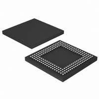
LPC3130FET180,551 NXP Semiconductors, LPC3130FET180,551 Datasheet - Page 52

LPC3130FET180,551
Manufacturer Part Number
LPC3130FET180,551
Description
IC ARM9 MCU 180MHZ 180-TFBGA
Manufacturer
NXP Semiconductors
Series
LPC3000r
Datasheet
1.OM11024.pdf
(72 pages)
Specifications of LPC3130FET180,551
Package / Case
180-TFBGA
Core Processor
ARM9
Core Size
32-Bit
Speed
180MHz
Connectivity
EBI/EMI, I²C, MMC, SPI, UART/USART, USB OTG
Peripherals
DMA, I²S, LCD, PWM, WDT
Program Memory Type
ROMless
Ram Size
96K x 8
Voltage - Supply (vcc/vdd)
1.1 V ~ 3.6 V
Data Converters
A/D 4x10b
Oscillator Type
External
Operating Temperature
-40°C ~ 85°C
Processor Series
LPC31
Core
ARM926EJ-S
Data Bus Width
16 bit, 32 bit
Data Ram Size
96 KB
Interface Type
I2C/I2S/UART/USB
Maximum Clock Frequency
180 MHz
Number Of Timers
4
Operating Supply Voltage
2.7 V to 3.6 V
Maximum Operating Temperature
+ 85 C
Mounting Style
SMD/SMT
3rd Party Development Tools
MDK-ARM, RL-ARM, ULINK2
Minimum Operating Temperature
- 40 C
On-chip Adc
4-ch x 10-bit
Cpu Family
LPC3000
Device Core
ARM926EJ-S
Device Core Size
16/32Bit
Frequency (max)
180MHz
Program Memory Size
Not Required
Total Internal Ram Size
96KB
Number Of Timers - General Purpose
4
Operating Supply Voltage (typ)
1.2/1.8/2.8/3.3/5V
Operating Supply Voltage (max)
1.3/3.6V
Operating Supply Voltage (min)
1/1.1/1.65/2.7V
Instruction Set Architecture
RISC
Operating Temp Range
-40C to 85C
Operating Temperature Classification
Industrial
Mounting
Surface Mount
Pin Count
180
Package Type
TFBGA
Package
180TFBGA
Family Name
LPC3000
Maximum Speed
180 MHz
Lead Free Status / RoHS Status
Lead free / RoHS Compliant
For Use With
568-4850 - KIT EVAL FOR LPC313X568-4062 - DEBUGGER J-LINK JTAG568-4061 - DEBUGGER U-LINK2 JTAG FOR NXP
Number Of I /o
-
Eeprom Size
-
Program Memory Size
-
Lead Free Status / Rohs Status
Lead free / RoHS Compliant
Other names
568-4696
935288013551
LPC3130FET180-S
935288013551
LPC3130FET180-S
Available stocks
Company
Part Number
Manufacturer
Quantity
Price
Company:
Part Number:
LPC3130FET180,551
Manufacturer:
NXP Semiconductors
Quantity:
10 000
NXP Semiconductors
Table 19.
T
[1]
[2]
[3]
[4]
[5]
[6]
LPC3130_3131
Preliminary data sheet
Symbol Parameter
f
T
t
t
t
t
t
t
t
t
t
t
t
oper
CLCX
CHCX
d(o)
h(o)
d(AV)
h(A)
d(QV)
h(Q)
su(D)
h(D)
QZ
amb
CLCL
Parameters are valid over operating temperature range unless otherwise specified.
All values valid for pads set to high slew rate. VDDE_IOA = VDDE_IOB = 1.8 ± 0.15 V. VDDI = 1.2 ± 0.1 V.
Refer to the LPC3130/3131 user manual for the programming of MPMCDynamicReadConfig and SYSCREG_MPMP_DELAYMODES
registers.
f
t
SYSCREG_MPMP_DELAYMODES register bits 11:6.
t
oper
d(o)
su(D)
=
−
, t
40
= 1 / T
, t
h(o)
h(D)
operating frequency
clock cycle time
clock LOW time
clock HIGH time
output delay time
output hold time
address valid delay
time
address hold time
data output valid
delay time
data output hold time
data input set-up
time
data input hold time
data output
high-impedance time
°
Dynamic characteristics of SDR SDRAM memory interface
, t
C to +85
d(AV)
times are dependent on SYSCREG_MPMP_DELAYMODES register bits 5:0.
CLCL
, t
9.3 SDRAM controller
h(A)
°
, t
C, unless otherwise specified; V
d(QV)
, t
h(Q)
times are dependent on MPMCDynamicReadConfig register value and
Conditions
on pin EBI_CKE
on pins
EBI_NRAS_BLOUT,
EBI_NCAS_BLOUT,
EBI_NWE,
EBI_NDYCS
on pins EBI_DQM_1,
EBI_DQM_0_NOE
on pin EBI_CKE
on pins
EBI_NRAS_BLOUT,
EBI_NCAS_BLOUT,
EBI_NWE,
EBI_NDYCS
on pins EBI_DQM_1,
EBI_DQM_0_NOE
All information provided in this document is subject to legal disclaimers.
Rev. 1.04 — 27 May 2010
DD(IO)
= 1.8 V and 3.3 V (SUP8).
[4]
[5]
[5]
[5]
[5]
[5]
[5]
[6]
[6]
Low-cost, low-power ARM926EJ-S microcontrollers
Min
-
11.1
-
-
-
-
-
0.13
−0.1
1.7
-
−0.1
-
4
<tbd>
<tbd>
-
Typical
80
<tbd>
5.55
5.55
-
-
-
-
-
-
-
-
-
-
-
-
-
[1][2][3]
LPC3130/3131
Max
90
-
-
-
3.6
3.6
5
3.6
3.6
5
5
5
9
10
-
-
<T
CLCL
© NXP B.V. 2010. All rights reserved.
52 of 72
Unit
MHz
ns
ns
ns
ns
ns
ns
ns
ns
ns
ns
ns
ns
ns
ns
ns
ns


