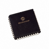
PIC18F442-I/L Microchip Technology, PIC18F442-I/L Datasheet - Page 188

PIC18F442-I/L
Manufacturer Part Number
PIC18F442-I/L
Description
IC MCU FLASH 8KX16 EE A/D 44PLCC
Manufacturer
Microchip Technology
Series
PIC® 18Fr
Datasheets
1.PIC16F616T-ISL.pdf
(8 pages)
2.PIC18F242-ISO.pdf
(332 pages)
3.PIC18F242-ISO.pdf
(14 pages)
4.PIC18F242-ISO.pdf
(16 pages)
5.PIC18F242-ISO.pdf
(16 pages)
6.PIC18F242-ISO.pdf
(14 pages)
7.PIC18LF242-ISO.pdf
(36 pages)
Specifications of PIC18F442-I/L
Core Size
8-Bit
Program Memory Size
16KB (8K x 16)
Core Processor
PIC
Speed
40MHz
Connectivity
I²C, SPI, UART/USART
Peripherals
Brown-out Detect/Reset, LVD, POR, PWM, WDT
Number Of I /o
34
Program Memory Type
FLASH
Eeprom Size
256 x 8
Ram Size
768 x 8
Voltage - Supply (vcc/vdd)
4.2 V ~ 5.5 V
Data Converters
A/D 8x10b
Oscillator Type
External
Operating Temperature
-40°C ~ 85°C
Package / Case
44-PLCC
Controller Family/series
PIC18
No. Of I/o's
34
Eeprom Memory Size
256Byte
Ram Memory Size
768Byte
Cpu Speed
40MHz
No. Of Timers
4
Processor Series
PIC18F
Core
PIC
Data Bus Width
8 bit
Data Ram Size
768 B
Interface Type
MSSP, SPI, I2C, PSP, USART
Maximum Clock Frequency
40 MHz
Number Of Programmable I/os
34
Number Of Timers
1 x 16 bit
Operating Supply Voltage
2 V to 5.5 V
Maximum Operating Temperature
+ 85 C
Mounting Style
SMD/SMT
3rd Party Development Tools
52715-96, 52716-328, 52717-734, 52712-325, EWPIC18
Development Tools By Supplier
PG164130, DV164035, DV244005, DV164005, PG164120, ICE2000, ICE4000, DM163022, DV164136
Minimum Operating Temperature
- 40 C
On-chip Adc
8
Package
44PLCC
Device Core
PIC
Family Name
PIC18
Maximum Speed
40 MHz
Lead Free Status / RoHS Status
Lead free / RoHS Compliant
For Use With
AC164309 - MODULE SKT FOR PM3 44PLCCXLT44L2 - SOCKET TRAN ICE 44PLCC444-1001 - DEMO BOARD FOR PICMICRO MCUDVA16XL441 - ADAPTER DEVICE ICE 44PLCCDV007003 - PROGRAMMER UNIVERSAL PROMATE II
Lead Free Status / Rohs Status
Details
Other names
PIC18F442I/L
Available stocks
Company
Part Number
Manufacturer
Quantity
Price
Company:
Part Number:
PIC18F442-I/L
Manufacturer:
Microchip Technology
Quantity:
10 000
- PIC16F616T-ISL PDF datasheet
- PIC18F242-ISO PDF datasheet #2
- PIC18F242-ISO PDF datasheet #3
- PIC18F242-ISO PDF datasheet #4
- PIC18F242-ISO PDF datasheet #5
- PIC18F242-ISO PDF datasheet #6
- PIC18LF242-ISO PDF datasheet #7
- Current page: 188 of 332
- Download datasheet (6Mb)
PIC18FXX2
17.2
The A/D conversion time per bit is defined as T
A/D conversion requires 12 T
The source of the A/D conversion clock is software
selectable. The seven possible options for T
• 2 T
• 4 T
• 8 T
• 16 T
• 32 T
• 64 T
• Internal A/D module RC oscillator (2-6 s)
For correct A/D conversions, the A/D conversion clock
(T
of 1.6 s.
Table 17-1 shows the resultant T
the device operating frequencies and the A/D clock
source selected.
TABLE 17-1:
DS39564C-page 186
AD
) must be selected to ensure a minimum T
OSC
OSC
OSC
OSC
OSC
OSC
Selecting the A/D Conversion Clock
Operation
16 T
32 T
64 T
2 T
4 T
8 T
RC
OSC
OSC
OSC
OSC
OSC
OSC
AD Clock Source (T
T
AD
vs. DEVICE OPERATING FREQUENCIES
AD
per 10-bit conversion.
AD
times derived from
ADCS2:ADCS0
AD
)
000
100
001
101
010
110
011
AD
AD
AD
are:
. The
time
17.3
The ADCON1, TRISA and TRISE registers control the
operation of the A/D port pins. The port pins that are
desired as analog inputs, must have their corresponding
TRIS bits set (input). If the TRIS bit is cleared (output),
the digital output level (V
The A/D operation is independent of the state of the
CHS2:CHS0 bits and the TRIS bits.
Note 1: When reading the port register, all pins con-
PIC18FXX2
10.00 MHz
20.00 MHz
40.00 MHz
1.25 MHz
2.50 MHz
5.00 MHz
Configuring Analog Port Pins
—
2: Analog levels on any pin that is defined as
Maximum Device Frequency
figured as analog input channels will read
as cleared (a low level). Pins configured as
digital inputs will convert an analog input.
Analog levels on a digitally configured input
will not affect the conversion accuracy.
a digital input (including the AN4:AN0
pins) may cause the input buffer to con-
sume current that is out of the device’s
specification.
© 2006 Microchip Technology Inc.
OH
or V
OL
PIC18LFXX2
) will be converted.
10.67 MHz
21.33 MHz
1.33 MHz
2.67 MHz
5.33 MHz
666 kHz
—
Related parts for PIC18F442-I/L
Image
Part Number
Description
Manufacturer
Datasheet
Request
R

Part Number:
Description:
IC, 8BIT MCU, PIC18F, 40MHZ, LCC-44
Manufacturer:
Microchip Technology
Datasheet:

Part Number:
Description:
IC, 8BIT MCU, PIC18LF, 40MHZ, PLCC-64
Manufacturer:
Microchip Technology
Datasheet:

Part Number:
Description:
IC, 8BIT MCU, PIC18F, 64MHZ, TQFP-80
Manufacturer:
Microchip Technology
Datasheet:

Part Number:
Description:
MCU, MPU & DSP Development Tools CAN/LIN PICtail Plus Daughter Board
Manufacturer:
Microchip Technology
Datasheet:

Part Number:
Description:
IC, 8BIT MCU, PIC18F, 64MHZ, DIP-40
Manufacturer:
Microchip Technology
Datasheet:

Part Number:
Description:
IC, 8BIT MCU, PIC18LF, 40MHZ, PLCC-64
Manufacturer:
Microchip Technology
Datasheet:

Part Number:
Description:
IC, 8BIT MCU, PIC18F, 64MHZ, TQFP-64
Manufacturer:
Microchip Technology

Part Number:
Description:
IC, 8BIT MCU, PIC18F, 64MHZ, TQFP-80
Manufacturer:
Microchip Technology

Part Number:
Description:
8KB, Flash, 768bytes-RAM, 36I/O, 8-bit Family,nanowatt XLP 40 UQFN 5x5x0.5mm TUB
Manufacturer:
Microchip Technology
Datasheet:

Part Number:
Description:
8KB, Flash, 768bytes-RAM, 36I/O, 8-bit Family,nanowatt XLP 40 UQFN 5x5x0.5mm TUB
Manufacturer:
Microchip Technology

Part Number:
Description:
16KB, Flash, 768bytes-RAM, 36I/O, 8-bit Family,nanowatt XLP 40 UQFN 5x5x0.5mm TU
Manufacturer:
Microchip Technology
Datasheet:

Part Number:
Description:
16KB, Flash, 768bytes-RAM, 36I/O, 8-bit Family,nanowatt XLP 40 UQFN 5x5x0.5mm TU
Manufacturer:
Microchip Technology

Part Number:
Description:
32KB, Flash, 1536bytes-RAM, 36I/O, 8-bit Family,nanowatt XLP 40 UQFN 5x5x0.5mm T
Manufacturer:
Microchip Technology
Datasheet:

Part Number:
Description:
32KB, Flash, 1536bytes-RAM, 36I/O, 8-bit Family,nanowatt XLP 40 UQFN 5x5x0.5mm T
Manufacturer:
Microchip Technology

Part Number:
Description:
64KB, Flash, 3968bytes-RAM, 36I/O, 8-bit Family,nanowatt XLP 40 UQFN 5x5x0.5mm T
Manufacturer:
Microchip Technology
Datasheet:


