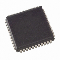
ATMEGA8535L-8JU Atmel, ATMEGA8535L-8JU Datasheet - Page 64

ATMEGA8535L-8JU
Manufacturer Part Number
ATMEGA8535L-8JU
Description
MCU AVR 8K ISP FLASH MEM 44-PLCC
Manufacturer
Atmel
Series
AVR® ATmegar
Specifications of ATMEGA8535L-8JU
Core Processor
AVR
Core Size
8-Bit
Speed
8MHz
Connectivity
I²C, SPI, UART/USART
Peripherals
Brown-out Detect/Reset, POR, PWM, WDT
Number Of I /o
32
Program Memory Size
8KB (4K x 16)
Program Memory Type
FLASH
Eeprom Size
512 x 8
Ram Size
512 x 8
Voltage - Supply (vcc/vdd)
2.7 V ~ 5.5 V
Data Converters
A/D 8x10b
Oscillator Type
Internal
Operating Temperature
-40°C ~ 85°C
Package / Case
44-PLCC
Processor Series
ATMEGA8x
Core
AVR8
Data Bus Width
8 bit
Data Ram Size
512 B
Interface Type
2-Wire, SPI, USART
Maximum Clock Frequency
8 MHz
Number Of Programmable I/os
32
Number Of Timers
3
Maximum Operating Temperature
+ 85 C
Mounting Style
SMD/SMT
3rd Party Development Tools
EWAVR, EWAVR-BL
Minimum Operating Temperature
- 40 C
On-chip Adc
10 bit, 8 Channel
Cpu Family
ATmega
Device Core
AVR
Device Core Size
8b
Frequency (max)
8MHz
Total Internal Ram Size
512Byte
# I/os (max)
32
Number Of Timers - General Purpose
3
Operating Supply Voltage (typ)
3.3/5V
Operating Supply Voltage (max)
5.5V
Operating Supply Voltage (min)
2.7V
Instruction Set Architecture
RISC
Operating Temp Range
-40C to 85C
Operating Temperature Classification
Industrial
Mounting
Surface Mount
Pin Count
44
Package Type
PLCC
For Use With
ATSTK600 - DEV KIT FOR AVR/AVR32770-1007 - ISP 4PORT ATMEL AVR MCU SPI/JTAGATAVRISP2 - PROGRAMMER AVR IN SYSTEMATSTK500 - PROGRAMMER AVR STARTER KIT
Lead Free Status / RoHS Status
Lead free / RoHS Compliant
Available stocks
Company
Part Number
Manufacturer
Quantity
Price
- Current page: 64 of 321
- Download datasheet (3Mb)
Alternate Functions of Port D
64
ATmega8535(L)
Table 31. Overriding Signals for Alternate Functions in PC1..PC0
Note:
The Port D pins with alternate functions are shown in Table 32.
Table 32. Port D Pins Alternate Functions
The alternate pin configuration is as follows:
• OC2 – Port D, Bit 7
OC2, Timer/Counter2 Output Compare Match output: The PD7 pin can serve as an
external output for the Timer/Counter2 Output Compare. The pin has to be configured
as an output (DDD7 set (one)) to serve this function. The OC2 pin is also the output pin
for the PWM mode timer function.
• ICP1 – Port D, Bit 6
ICP1 – Input Capture Pin: The PD6 pin can act as an Input Capture pin for
Timer/Counter1.
• OC1A – Port D, Bit 5
OC1A, Output Compare Match A output: The PD5 pin can serve as an external output
for the Timer/Counter1 Output Compare A. The pin has to be configured as an output
Signal Name
PUOE
PUOV
DDOE
DDOV
PVOE
PVOV
DIEOE
DIEOV
DI
AIO
Port Pin
PD7
PD6
PD5
PD4
PD3
PD2
PD1
PD0
1. When enabled, the Two-wire Serial Interface enables slew-rate controls on the output
pins PC0 and PC1. This is not shown in the figure. In addition, spike filters are con-
nected between the AIO outputs shown in the port figure and the digital logic of the
TWI module.
Alternate Function
OC2 (Timer/Counter2 Output Compare Match Output)
ICP1 (Timer/Counter1 Input Capture Pin)
OC1A (Timer/Counter1 Output Compare A Match Output)
OC1B (Timer/Counter1 Output Compare B Match Output)
INT1 (External Interrupt 1 Input)
INT0 (External Interrupt 0 Input)
TXD (USART Output Pin)
RXD (USART Input Pin)
PC1/SDA
TWEN
PORTC1 • PUD
TWEN
SDA_OUT
TWEN
0
0
0
–
SDA INPUT
PC0/SCL
TWEN
PORTC0 • PUD
TWEN
SCL_OUT
TWEN
0
0
0
–
SCL INPUT
(1)
2502K–AVR–10/06
Related parts for ATMEGA8535L-8JU
Image
Part Number
Description
Manufacturer
Datasheet
Request
R

Part Number:
Description:
IC AVR MCU 2.4GHZ XCEIVER 64QFN
Manufacturer:
Atmel
Datasheet:

Part Number:
Description:
Manufacturer:
Atmel
Datasheet:

Part Number:
Description:
MCU ATMEGA644/AT86RF230 40-DIP
Manufacturer:
Atmel
Datasheet:

Part Number:
Description:
BUNDLE ATMEGA644P/AT86RF230 QFN
Manufacturer:
Atmel
Datasheet:

Part Number:
Description:
BUNDLE ATMEGA644P/AT86RF230 TQFP
Manufacturer:
Atmel
Datasheet:

Part Number:
Description:
MCU ATMEGA1281/AT86RF230 64-TQFP
Manufacturer:
Atmel
Datasheet:

Part Number:
Description:
MCU ATMEGA1280/AT86RF230 100TQFP
Manufacturer:
Atmel
Datasheet:

Part Number:
Description:
BUNDLE ATMEGA1280/AT86RF100-TQFP
Manufacturer:
Atmel
Datasheet:

Part Number:
Description:
BUNDLE ATMEGA2560V/AT86RF230-ZU
Manufacturer:
Atmel
Datasheet:

Part Number:
Description:
MCU ATMEGA2561/AT86RF230 64-TQFP
Manufacturer:
Atmel
Datasheet:

Part Number:
Description:
INTERVAL AND WIPE/WASH WIPER CONTROL IC WITH DELAY
Manufacturer:
ATMEL Corporation
Datasheet:

Part Number:
Description:
Low-Voltage Voice-Switched IC for Hands-Free Operation
Manufacturer:
ATMEL Corporation
Datasheet:

Part Number:
Description:
MONOLITHIC INTEGRATED FEATUREPHONE CIRCUIT
Manufacturer:
ATMEL Corporation
Datasheet:

Part Number:
Description:
AM-FM Receiver IC U4255BM-M
Manufacturer:
ATMEL Corporation
Datasheet:


