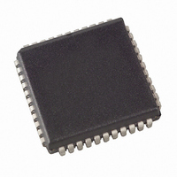
ATMEGA8535L-8JU Atmel, ATMEGA8535L-8JU Datasheet - Page 107

ATMEGA8535L-8JU
Manufacturer Part Number
ATMEGA8535L-8JU
Description
MCU AVR 8K ISP FLASH MEM 44-PLCC
Manufacturer
Atmel
Series
AVR® ATmegar
Specifications of ATMEGA8535L-8JU
Core Processor
AVR
Core Size
8-Bit
Speed
8MHz
Connectivity
I²C, SPI, UART/USART
Peripherals
Brown-out Detect/Reset, POR, PWM, WDT
Number Of I /o
32
Program Memory Size
8KB (4K x 16)
Program Memory Type
FLASH
Eeprom Size
512 x 8
Ram Size
512 x 8
Voltage - Supply (vcc/vdd)
2.7 V ~ 5.5 V
Data Converters
A/D 8x10b
Oscillator Type
Internal
Operating Temperature
-40°C ~ 85°C
Package / Case
44-PLCC
Processor Series
ATMEGA8x
Core
AVR8
Data Bus Width
8 bit
Data Ram Size
512 B
Interface Type
2-Wire, SPI, USART
Maximum Clock Frequency
8 MHz
Number Of Programmable I/os
32
Number Of Timers
3
Maximum Operating Temperature
+ 85 C
Mounting Style
SMD/SMT
3rd Party Development Tools
EWAVR, EWAVR-BL
Minimum Operating Temperature
- 40 C
On-chip Adc
10 bit, 8 Channel
Cpu Family
ATmega
Device Core
AVR
Device Core Size
8b
Frequency (max)
8MHz
Total Internal Ram Size
512Byte
# I/os (max)
32
Number Of Timers - General Purpose
3
Operating Supply Voltage (typ)
3.3/5V
Operating Supply Voltage (max)
5.5V
Operating Supply Voltage (min)
2.7V
Instruction Set Architecture
RISC
Operating Temp Range
-40C to 85C
Operating Temperature Classification
Industrial
Mounting
Surface Mount
Pin Count
44
Package Type
PLCC
For Use With
ATSTK600 - DEV KIT FOR AVR/AVR32770-1007 - ISP 4PORT ATMEL AVR MCU SPI/JTAGATAVRISP2 - PROGRAMMER AVR IN SYSTEMATSTK500 - PROGRAMMER AVR STARTER KIT
Lead Free Status / RoHS Status
Lead free / RoHS Compliant
Available stocks
Company
Part Number
Manufacturer
Quantity
Price
- Current page: 107 of 321
- Download datasheet (3Mb)
2502K–AVR–10/06
In phase and frequency correct PWM mode the counter is incremented until the counter
value matches either the value in ICR1 (WGM13:0 = 8), or the value in OCR1A
(WGM13:0 = 9). The counter has then reached the TOP and changes the count direc-
tion. The TCNT1 value will be equal to TOP for one timer clock cycle. The timing
diagram for the phase correct and frequency correct PWM mode is shown in Figure 48.
The figure shows phase and frequency correct PWM mode when OCR1A or ICR1 is
used to define TOP. The TCNT1 value is in the timing diagram shown as a histogram for
illustrating the dual-slope operation. The diagram includes non-inverted and inverted
PWM outputs. The small horizontal line marks on the TCNT1 slopes represent compare
matches between OCR1x and TCNT1. The OC1x Interrupt Flag will be set when a Com-
pare Match occurs.
Figure 48. Phase and Frequency Correct PWM Mode, Timing Diagram
The Timer/Counter Overflow Flag (TOV1) is set at the same timer clock cycle as the
OCR1x Registers are updated with the double buffer value (at BOTTOM). When either
OCR1A or ICR1 is used for defining the TOP value, the OC1A or ICF1 Flag set when
TCNT1 has reached TOP. The interrupt flags can then be used to generate an interrupt
each time the counter reaches the TOP or BOTTOM value.
When changing the TOP value the program must ensure that the new TOP value is
higher or equal to the value of all of the compare registers. If the TOP value is lower
than any of the compare registers, a Compare Match will never occur between the
TCNT1 and the OCR1x.
As Figure 48 shows the output generated is, in contrast to the phase correct mode, sym-
metrical in all periods. Since the OCR1x Registers are updated at BOTTOM, the length
of the rising and the falling slopes will always be equal. This gives symmetrical output
pulses and the frequency is, therefore, correct.
Using the ICR1 Register for defining TOP works well when using fixed TOP values. By
using ICR1, the OCR1A Register is free to be used for generating a PWM output on
OC1A. However, if the base PWM frequency is actively changed by changing the TOP
value, using the OCR1A as TOP is clearly a better choice due to its double buffer
feature.
TCNTn
OCnx
OCnx
Period
1
2
3
4
ATmega8535(L)
OCnA Interrupt Flag Set
or ICFn Interrupt Flag Set
(Interrupt on TOP)
OCRnx/TOP Update and
TOVn Interrupt Flag Set
(Interrupt on Bottom)
(COMnx1:0 = 2)
(COMnx1:0 = 3)
107
Related parts for ATMEGA8535L-8JU
Image
Part Number
Description
Manufacturer
Datasheet
Request
R

Part Number:
Description:
IC AVR MCU 2.4GHZ XCEIVER 64QFN
Manufacturer:
Atmel
Datasheet:

Part Number:
Description:
Manufacturer:
Atmel
Datasheet:

Part Number:
Description:
MCU ATMEGA644/AT86RF230 40-DIP
Manufacturer:
Atmel
Datasheet:

Part Number:
Description:
BUNDLE ATMEGA644P/AT86RF230 QFN
Manufacturer:
Atmel
Datasheet:

Part Number:
Description:
BUNDLE ATMEGA644P/AT86RF230 TQFP
Manufacturer:
Atmel
Datasheet:

Part Number:
Description:
MCU ATMEGA1281/AT86RF230 64-TQFP
Manufacturer:
Atmel
Datasheet:

Part Number:
Description:
MCU ATMEGA1280/AT86RF230 100TQFP
Manufacturer:
Atmel
Datasheet:

Part Number:
Description:
BUNDLE ATMEGA1280/AT86RF100-TQFP
Manufacturer:
Atmel
Datasheet:

Part Number:
Description:
BUNDLE ATMEGA2560V/AT86RF230-ZU
Manufacturer:
Atmel
Datasheet:

Part Number:
Description:
MCU ATMEGA2561/AT86RF230 64-TQFP
Manufacturer:
Atmel
Datasheet:

Part Number:
Description:
INTERVAL AND WIPE/WASH WIPER CONTROL IC WITH DELAY
Manufacturer:
ATMEL Corporation
Datasheet:

Part Number:
Description:
Low-Voltage Voice-Switched IC for Hands-Free Operation
Manufacturer:
ATMEL Corporation
Datasheet:

Part Number:
Description:
MONOLITHIC INTEGRATED FEATUREPHONE CIRCUIT
Manufacturer:
ATMEL Corporation
Datasheet:

Part Number:
Description:
AM-FM Receiver IC U4255BM-M
Manufacturer:
ATMEL Corporation
Datasheet:


