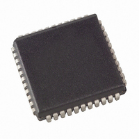
ATMEGA8535L-8JU Atmel, ATMEGA8535L-8JU Datasheet - Page 218

ATMEGA8535L-8JU
Manufacturer Part Number
ATMEGA8535L-8JU
Description
MCU AVR 8K ISP FLASH MEM 44-PLCC
Manufacturer
Atmel
Series
AVR® ATmegar
Specifications of ATMEGA8535L-8JU
Core Processor
AVR
Core Size
8-Bit
Speed
8MHz
Connectivity
I²C, SPI, UART/USART
Peripherals
Brown-out Detect/Reset, POR, PWM, WDT
Number Of I /o
32
Program Memory Size
8KB (4K x 16)
Program Memory Type
FLASH
Eeprom Size
512 x 8
Ram Size
512 x 8
Voltage - Supply (vcc/vdd)
2.7 V ~ 5.5 V
Data Converters
A/D 8x10b
Oscillator Type
Internal
Operating Temperature
-40°C ~ 85°C
Package / Case
44-PLCC
Processor Series
ATMEGA8x
Core
AVR8
Data Bus Width
8 bit
Data Ram Size
512 B
Interface Type
2-Wire, SPI, USART
Maximum Clock Frequency
8 MHz
Number Of Programmable I/os
32
Number Of Timers
3
Maximum Operating Temperature
+ 85 C
Mounting Style
SMD/SMT
3rd Party Development Tools
EWAVR, EWAVR-BL
Minimum Operating Temperature
- 40 C
On-chip Adc
10 bit, 8 Channel
Cpu Family
ATmega
Device Core
AVR
Device Core Size
8b
Frequency (max)
8MHz
Total Internal Ram Size
512Byte
# I/os (max)
32
Number Of Timers - General Purpose
3
Operating Supply Voltage (typ)
3.3/5V
Operating Supply Voltage (max)
5.5V
Operating Supply Voltage (min)
2.7V
Instruction Set Architecture
RISC
Operating Temp Range
-40C to 85C
Operating Temperature Classification
Industrial
Mounting
Surface Mount
Pin Count
44
Package Type
PLCC
For Use With
ATSTK600 - DEV KIT FOR AVR/AVR32770-1007 - ISP 4PORT ATMEL AVR MCU SPI/JTAGATAVRISP2 - PROGRAMMER AVR IN SYSTEMATSTK500 - PROGRAMMER AVR STARTER KIT
Lead Free Status / RoHS Status
Lead free / RoHS Compliant
Available stocks
Company
Part Number
Manufacturer
Quantity
Price
- Current page: 218 of 321
- Download datasheet (3Mb)
ADC Conversion Result
218
ATmega8535(L)
After the conversion is complete (ADIF is high), the conversion result can be found in
the ADC Result Registers (ADCL, ADCH).
For single ended conversion, the result is
where V
ence (see Table 84 on page 219 and Table 85 on page 220). 0x000 represents analog
ground, and 0x3FF represents the selected reference voltage minus one LSB.
If differential channels are used, the result is
where V
input pin, GAIN the selected gain factor, and V
result is presented in two’s complement form, from 0x200 (-512d) through 0x1FF
(+511d). Note that if the user wants to perform a quick polarity check of the results, it is
sufficient to read the MSB of the result (ADC9 in ADCH). If the bit is one, the result is
negative, and if the bit is zero, the result is positive. Figure 111 shows the decoding of
the differential input range.
Table 83 shows the resulting output codes if the differential input channel pair (ADCn -
ADCm) is selected with a gain of GAIN and a reference voltage of V
Figure 111. Differential Measurement Range
- V
REF
/GAIN
IN
POS
is the voltage on the selected input pin and V
is the voltage on the positive input pin, V
ADC
=
(
----------------------------------------------------------------------- -
Output Code
V
0x3FF
POS
0x1FF
0x000
ADC
–
0
V
0x200
NEG
=
V
REF
V
--------------------------
) GAIN 512
IN
⋅
V
⋅
REF
REF
1024
the selected voltage reference. The
⋅
NEG
REF
the voltage on the negative
the selected voltage refer-
V
REF
REF
/GAIN Differential Input
.
Voltage (Volts)
2502K–AVR–10/06
Related parts for ATMEGA8535L-8JU
Image
Part Number
Description
Manufacturer
Datasheet
Request
R

Part Number:
Description:
IC AVR MCU 2.4GHZ XCEIVER 64QFN
Manufacturer:
Atmel
Datasheet:

Part Number:
Description:
Manufacturer:
Atmel
Datasheet:

Part Number:
Description:
MCU ATMEGA644/AT86RF230 40-DIP
Manufacturer:
Atmel
Datasheet:

Part Number:
Description:
BUNDLE ATMEGA644P/AT86RF230 QFN
Manufacturer:
Atmel
Datasheet:

Part Number:
Description:
BUNDLE ATMEGA644P/AT86RF230 TQFP
Manufacturer:
Atmel
Datasheet:

Part Number:
Description:
MCU ATMEGA1281/AT86RF230 64-TQFP
Manufacturer:
Atmel
Datasheet:

Part Number:
Description:
MCU ATMEGA1280/AT86RF230 100TQFP
Manufacturer:
Atmel
Datasheet:

Part Number:
Description:
BUNDLE ATMEGA1280/AT86RF100-TQFP
Manufacturer:
Atmel
Datasheet:

Part Number:
Description:
BUNDLE ATMEGA2560V/AT86RF230-ZU
Manufacturer:
Atmel
Datasheet:

Part Number:
Description:
MCU ATMEGA2561/AT86RF230 64-TQFP
Manufacturer:
Atmel
Datasheet:

Part Number:
Description:
INTERVAL AND WIPE/WASH WIPER CONTROL IC WITH DELAY
Manufacturer:
ATMEL Corporation
Datasheet:

Part Number:
Description:
Low-Voltage Voice-Switched IC for Hands-Free Operation
Manufacturer:
ATMEL Corporation
Datasheet:

Part Number:
Description:
MONOLITHIC INTEGRATED FEATUREPHONE CIRCUIT
Manufacturer:
ATMEL Corporation
Datasheet:

Part Number:
Description:
AM-FM Receiver IC U4255BM-M
Manufacturer:
ATMEL Corporation
Datasheet:


