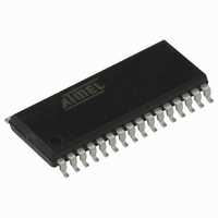
AT90PWM3B-16SU Atmel, AT90PWM3B-16SU Datasheet - Page 122

AT90PWM3B-16SU
Manufacturer Part Number
AT90PWM3B-16SU
Description
IC MCU AVR RISC 8K FLASH 32-SOIC
Manufacturer
Atmel
Series
AVR® 90PWM Lightingr
Specifications of AT90PWM3B-16SU
Core Processor
AVR
Core Size
8-Bit
Speed
16MHz
Connectivity
SPI, UART/USART
Peripherals
Brown-out Detect/Reset, POR, PWM, WDT
Number Of I /o
27
Program Memory Size
8KB (8K x 8)
Program Memory Type
FLASH
Eeprom Size
512 x 8
Ram Size
512 x 8
Voltage - Supply (vcc/vdd)
2.7 V ~ 5.5 V
Data Converters
A/D 11x10b; D/A 1x10b
Oscillator Type
Internal
Operating Temperature
-40°C ~ 105°C
Package / Case
32-SOIC (7.5mm Width)
Processor Series
AT90PWMx
Core
AVR8
Data Bus Width
8 bit
Data Ram Size
512 B
Interface Type
SPI/USART
Maximum Clock Frequency
16 MHz
Number Of Programmable I/os
27
Number Of Timers
2
Operating Supply Voltage
2.7 V to 5.5 V
Maximum Operating Temperature
+ 105 C
Mounting Style
SMD/SMT
3rd Party Development Tools
EWAVR, EWAVR-BL
Development Tools By Supplier
ATAVRDRAGON, ATSTK500, ATSTK600, ATAVRISP2, ATAVRONEKIT, ATAVRFBKIT, ATAVRISP2
Minimum Operating Temperature
- 40 C
On-chip Adc
11-ch x 10-bit
On-chip Dac
1-chx10-bit
Controller Family/series
AVR PWM
Eeprom Memory Size
512Byte
Ram Memory Size
512Byte
Cpu Speed
16MHz
Rohs Compliant
Yes
For Use With
ATSTK600-SOIC - STK600 SOCKET/ADAPTER FOR SOIC770-1007 - ISP 4PORT ATMEL AVR MCU SPI/JTAGATAVRMC200 - KIT EVAL FOR AT90PWM3 ASYNCATAVRFBKIT - KIT DEMO BALLAST FOR AT90PWM2ATAVRISP2 - PROGRAMMER AVR IN SYSTEMATSTK520 - ADAPTER KIT FOR 90PWM
Lead Free Status / RoHS Status
Lead free / RoHS Compliant
Available stocks
Company
Part Number
Manufacturer
Quantity
Price
Company:
Part Number:
AT90PWM3B-16SU
Manufacturer:
Atmel
Quantity:
4 000
Part Number:
AT90PWM3B-16SU
Manufacturer:
MICROCHIP/微芯
Quantity:
20 000
- Current page: 122 of 361
- Download datasheet (7Mb)
15.10 16-bit Timer/Counter Register Description
15.10.1
122
AT90PWM2/3/2B/3B
Timer/Counter1 Control Register A – TCCR1A
Figure 15-12. Timer/Counter Timing Diagram, no Prescaling
Figure 15-13
Figure 15-13. Timer/Counter Timing Diagram, with Prescaler (f
• Bit 7:6 – COMnA1:0: Compare Output Mode for Channel A
• Bit 5:4 – COMnB1:0: Compare Output Mode for Channel B
The COMnA1:0 and COMnB1:0 control the Output Compare pins (OCnA and OCnB respec-
tively) behavior. If one or both of the COMnA1:0 bits are written to one, the OCnA output
overrides the normal port functionality of the I/O pin it is connected to. If one or both of the
COMnB1:0 bit are written to one, the OCnB output overrides the normal port functionality of the
Bit
Read/Write
Initial Value
and ICF n
(PC and PFC PWM)
and ICFn
(CTC and FPWM)
TOVn
(Update at TOP)
(PC and PFC PWM)
TOVn
(CTC and FPWM)
(Update at TOP)
TCNTn
TCNTn
OCRnx
as TOP)
(clk
TCNTn
TCNTn
OCRnx
(clk
as TOP)
clk
clk
clk
clk
I/O
(FPWM)
I/O
shows the same timing data, but with the prescaler enabled.
(FPWM)
I/O
Tn
I/O
Tn
/8)
COM1A1
(if used
/1)
(if used
R/W
7
0
COM1A0
R/W
6
0
TOP - 1
TOP - 1
TOP - 1
TOP - 1
Old OCRnx Value
Old OCRnx Value
COM1B1
R/W
5
0
COM1B0
R/W
4
0
TOP
TOP
TOP
TOP
R
3
–
0
BOTTOM
BOTTOM
TOP - 1
TOP - 1
clk_I/O
R
2
0
–
New OCRnx Value
New OCRnx Value
/8)
WGM11
R/W
1
0
BOTTOM + 1
BOTTOM + 1
TOP - 2
TOP - 2
WGM10
R/W
0
0
4317J–AVR–08/10
TCCR1A
Related parts for AT90PWM3B-16SU
Image
Part Number
Description
Manufacturer
Datasheet
Request
R

Part Number:
Description:
Manufacturer:
Atmel Corporation
Datasheet:

Part Number:
Description:
IC MCU AVR RISC 8K FLASH 32-QFN
Manufacturer:
Atmel
Datasheet:

Part Number:
Description:
MCU AVR 8K FLASH 16MHA 32SOIC
Manufacturer:
Atmel
Datasheet:

Part Number:
Description:
IC AVR MCU FLASH 8K 32QFN
Manufacturer:
Atmel
Datasheet:

Part Number:
Description:
IC AVR MCU FLASH 8K 32SOIC
Manufacturer:
Atmel
Datasheet:

Part Number:
Description:
MCU AVR 8K FLASH 16MHZ 32-QFN
Manufacturer:
Atmel
Datasheet:

Part Number:
Description:
DEV KIT FOR AVR/AVR32
Manufacturer:
Atmel
Datasheet:

Part Number:
Description:
INTERVAL AND WIPE/WASH WIPER CONTROL IC WITH DELAY
Manufacturer:
ATMEL Corporation
Datasheet:

Part Number:
Description:
Low-Voltage Voice-Switched IC for Hands-Free Operation
Manufacturer:
ATMEL Corporation
Datasheet:

Part Number:
Description:
MONOLITHIC INTEGRATED FEATUREPHONE CIRCUIT
Manufacturer:
ATMEL Corporation
Datasheet:

Part Number:
Description:
AM-FM Receiver IC U4255BM-M
Manufacturer:
ATMEL Corporation
Datasheet:

Part Number:
Description:
Monolithic Integrated Feature Phone Circuit
Manufacturer:
ATMEL Corporation
Datasheet:

Part Number:
Description:
Multistandard Video-IF and Quasi Parallel Sound Processing
Manufacturer:
ATMEL Corporation
Datasheet:


