ATTINY13-20MU Atmel, ATTINY13-20MU Datasheet - Page 65
ATTINY13-20MU
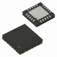
Manufacturer Part Number
ATTINY13-20MU
Description
IC MCU AVR 1K FLASH 10MHZ 20-MLF
Manufacturer
Atmel
Series
AVR® ATtinyr
Specifications of ATTINY13-20MU
Core Processor
AVR
Core Size
8-Bit
Speed
20MHz
Peripherals
Brown-out Detect/Reset, POR, PWM, WDT
Number Of I /o
6
Program Memory Size
1KB (512 x 16)
Program Memory Type
FLASH
Eeprom Size
64 x 8
Ram Size
64 x 8
Voltage - Supply (vcc/vdd)
2.7 V ~ 5.5 V
Data Converters
A/D 4x10b
Oscillator Type
Internal
Operating Temperature
-40°C ~ 85°C
Package / Case
20-MLF®, QFN
Processor Series
ATTINY1x
Core
AVR8
Data Bus Width
8 bit
Data Ram Size
64 B
Interface Type
SPI
Maximum Clock Frequency
20 MHz
Number Of Programmable I/os
6
Number Of Timers
2
Operating Supply Voltage
2.7 V to 5.5 V
Maximum Operating Temperature
+ 85 C
Mounting Style
SMD/SMT
3rd Party Development Tools
EWAVR, EWAVR-BL
Development Tools By Supplier
ATAVRDRAGON, ATSTK500, ATSTK600, ATAVRISP2, ATAVRONEKIT, ATAKSTK511
Minimum Operating Temperature
- 40 C
On-chip Adc
10 bit, 4 Channel
Package
20MLF EP
Device Core
AVR
Family Name
ATtiny
Maximum Speed
20 MHz
For Use With
ATSTK600-DIP40 - STK600 SOCKET/ADAPTER 40-PDIP770-1007 - ISP 4PORT ATMEL AVR MCU SPI/JTAGATAVRDRAGON - KIT DRAGON 32KB FLASH MEM AVRATAVRISP2 - PROGRAMMER AVR IN SYSTEMATJTAGICE2 - AVR ON-CHIP D-BUG SYSTEM
Lead Free Status / RoHS Status
Lead free / RoHS Compliant
Connectivity
-
Lead Free Status / Rohs Status
Details


2535J–AVR–08/10
for power regulation, rectification, and DAC applications. High frequency allows physically small
sized external components (coils, capacitors), and therefore reduces total system cost.
In fast PWM mode, the counter is incremented until the counter value matches the TOP value.
The counter is then cleared at the following timer clock cycle. The timing diagram for the fast
PWM mode is shown in
shown as a histogram for illustrating the single-slope operation. The diagram includes non-
inverted and inverted PWM outputs. The small horizontal line marks on the TCNT0 slopes repre-
sent Compare Matches between OCR0x and TCNT0.
Figure 11-6. Fast PWM Mode, Timing Diagram
The Timer/Counter Overflow Flag (TOV0) is set each time the counter reaches TOP. If the inter-
rupt is enabled, the interrupt handler routine can be used for updating the compare value.
In fast PWM mode, the compare unit allows generation of PWM waveforms on the OC0x pins.
Setting the COM0x1:0 bits to two will produce a non-inverted PWM and an inverted PWM output
can be generated by setting the COM0x1:0 to three: Setting the COM0A1:0 bits to one allows
the AC0A pin to toggle on Compare Matches if the WGM02 bit is set. This option is not available
for the OC0B pin (See
port pin if the data direction for the port pin is set as output. The PWM waveform is generated by
setting (or clearing) the OC0x Register at the Compare Match between OCR0x and TCNT0, and
clearing (or setting) the OC0x Register at the timer clock cycle the counter is cleared (changes
from TOP to BOTTOM).
The PWM frequency for the output can be calculated by the following equation:
The N variable represents the prescale factor (1, 8, 64, 256, or 1024).
The extreme values for the OCR0A Register represents special cases when generating a PWM
waveform output in the fast PWM mode. If the OCR0A is set equal to BOTTOM, the output will
be a narrow spike for each MAX+1 timer clock cycle. Setting the OCR0A equal to MAX will result
TCNTn
OCn
OCn
Period
1
Table 11-3 on page
2
Figure 11-6 on page
3
f
OCnxPWM
4
70). The actual OC0x value will only be visible on the
65. The TCNT0 value is in the timing diagram
5
=
------------------
N 256
f
clk_I/O
⋅
6
7
OCRnx Interrupt Flag Set
OCRnx Update and
TOVn Interrupt Flag Set
(COMnx1:0 = 2)
(COMnx1:0 = 3)
65
Related parts for ATTINY13-20MU
Image
Part Number
Description
Manufacturer
Datasheet
Request
R

Part Number:
Description:
IC MCU AVR 1K FLASH 20MHZ 8SOIC
Manufacturer:
Atmel
Datasheet:

Part Number:
Description:
Manufacturer:
Atmel Corporation
Datasheet:
Part Number:
Description:
IC MCU AVR 1K FLASH 20MHZ 8SOIC
Manufacturer:
Atmel
Datasheet:

Part Number:
Description:
IC MCU AVR 1K FLASH 20MHZ 8DIP
Manufacturer:
Atmel
Datasheet:

Part Number:
Description:
MCU AVR 1KB FLASH 20MHZ 3X3 QFN
Manufacturer:
Atmel
Datasheet:
Part Number:
Description:
IC MCU AVR 1K FLASH 20MHZ 8SOIC
Manufacturer:
Atmel
Datasheet:
Part Number:
Description:
IC MCU AVR 1K 5V 20MHZ 8DIP
Manufacturer:
Atmel
Datasheet:
Part Number:
Description:
IC MCU AVR 1K 5V 20MHZ 8SOIC
Manufacturer:
Atmel
Datasheet:
Part Number:
Description:
IC MCU AVR 1K 5V 20MHZ 8SOIC
Manufacturer:
Atmel
Datasheet:
Part Number:
Description:
IC MCU AVR 1K FLASH 20MHZ 8DIP
Manufacturer:
Atmel
Datasheet:
Part Number:
Description:
IC MCU AVR 1K FLASH 20MHZ 8SOIC
Manufacturer:
Atmel
Datasheet:
Part Number:
Description:
MCU AVR 1KB FLASH 20MHZ 8SOIC GW
Manufacturer:
Atmel
Datasheet: