ATTINY13-20MU Atmel, ATTINY13-20MU Datasheet - Page 59
ATTINY13-20MU
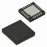
Manufacturer Part Number
ATTINY13-20MU
Description
IC MCU AVR 1K FLASH 10MHZ 20-MLF
Manufacturer
Atmel
Series
AVR® ATtinyr
Specifications of ATTINY13-20MU
Core Processor
AVR
Core Size
8-Bit
Speed
20MHz
Peripherals
Brown-out Detect/Reset, POR, PWM, WDT
Number Of I /o
6
Program Memory Size
1KB (512 x 16)
Program Memory Type
FLASH
Eeprom Size
64 x 8
Ram Size
64 x 8
Voltage - Supply (vcc/vdd)
2.7 V ~ 5.5 V
Data Converters
A/D 4x10b
Oscillator Type
Internal
Operating Temperature
-40°C ~ 85°C
Package / Case
20-MLF®, QFN
Processor Series
ATTINY1x
Core
AVR8
Data Bus Width
8 bit
Data Ram Size
64 B
Interface Type
SPI
Maximum Clock Frequency
20 MHz
Number Of Programmable I/os
6
Number Of Timers
2
Operating Supply Voltage
2.7 V to 5.5 V
Maximum Operating Temperature
+ 85 C
Mounting Style
SMD/SMT
3rd Party Development Tools
EWAVR, EWAVR-BL
Development Tools By Supplier
ATAVRDRAGON, ATSTK500, ATSTK600, ATAVRISP2, ATAVRONEKIT, ATAKSTK511
Minimum Operating Temperature
- 40 C
On-chip Adc
10 bit, 4 Channel
Package
20MLF EP
Device Core
AVR
Family Name
ATtiny
Maximum Speed
20 MHz
For Use With
ATSTK600-DIP40 - STK600 SOCKET/ADAPTER 40-PDIP770-1007 - ISP 4PORT ATMEL AVR MCU SPI/JTAGATAVRDRAGON - KIT DRAGON 32KB FLASH MEM AVRATAVRISP2 - PROGRAMMER AVR IN SYSTEMATJTAGICE2 - AVR ON-CHIP D-BUG SYSTEM
Lead Free Status / RoHS Status
Lead free / RoHS Compliant
Connectivity
-
Lead Free Status / Rohs Status
Details


11.2.1
11.2.2
11.3
11.4
2535J–AVR–08/10
Timer/Counter Clock Sources
Counter Unit
Registers
Definitions
The Timer/Counter (TCNT0) and Output Compare Registers (OCR0A and OCR0B) are 8-bit
registers. Interrupt request (abbreviated to Int.Req. in the figure) signals are all visible in the
Timer Interrupt Flag Register (TIFR0). All interrupts are individually masked with the Timer Inter-
rupt Mask Register (TIMSK0). TIFR0 and TIMSK0 are not shown in the figure.
The Timer/Counter can be clocked internally, via the prescaler, or by an external clock source on
the T0 pin. The Clock Select logic block controls which clock source and edge the Timer/Counter
uses to increment (or decrement) its value. The Timer/Counter is inactive when no clock source
is selected. The output from the Clock Select logic is referred to as the timer clock (clk
The double buffered Output Compare Registers (OCR0A and OCR0B) is compared with the
Timer/Counter value at all times. The result of the compare can be used by the Waveform Gen-
erator to generate a PWM or variable frequency output on the Output Compare pins (OC0A and
OC0B).
set the Compare Flag (OCF0A or OCF0B) which can be used to generate an Output Compare
interrupt request.
Many register and bit references in this section are written in general form. A lower case “n”
replaces the Timer/Counter number, in this case 0. A lower case “x” replaces the Output Com-
pare Unit, in this case Compare Unit A or Compare Unit B. However, when using the register or
bit defines in a program, the precise form must be used, i.e., TCNT0 for accessing
Timer/Counter0 counter value and so on.
The definitions in
Table 11-1.
The Timer/Counter can be clocked by an internal or an external clock source. The clock source
is selected by the Clock Select logic which is controlled by the Clock Select (CS02:0) bits
located in the Timer/Counter Control Register (TCCR0B). For details on clock sources and pres-
caler, see
The main part of the 8-bit Timer/Counter is the programmable bi-directional counter unit.
11-2
BOTTOM
MAX
TOP
shows a block diagram of the counter and its surroundings.
See “Output Compare Unit” on page 60.
“Timer/Counter Prescaler” on page
Definitions
The counter reaches the BOTTOM when it becomes 0x00.
The counter reaches its MAXimum when it becomes 0xFF (decimal 255).
The counter reaches the TOP when it becomes equal to the highest value in the
count sequence. The TOP value can be assigned to be the fixed value 0xFF
(MAX) or the value stored in the OCR0A Register. The assignment is depen-
dent on the mode of operation.
Table 11-1 on page 59
are also used extensively throughout the document.
76.
for details. The Compare Match event will also
T0
).
Figure
59
Related parts for ATTINY13-20MU
Image
Part Number
Description
Manufacturer
Datasheet
Request
R

Part Number:
Description:
IC MCU AVR 1K FLASH 20MHZ 8SOIC
Manufacturer:
Atmel
Datasheet:

Part Number:
Description:
Manufacturer:
Atmel Corporation
Datasheet:
Part Number:
Description:
IC MCU AVR 1K FLASH 20MHZ 8SOIC
Manufacturer:
Atmel
Datasheet:

Part Number:
Description:
IC MCU AVR 1K FLASH 20MHZ 8DIP
Manufacturer:
Atmel
Datasheet:

Part Number:
Description:
MCU AVR 1KB FLASH 20MHZ 3X3 QFN
Manufacturer:
Atmel
Datasheet:
Part Number:
Description:
IC MCU AVR 1K FLASH 20MHZ 8SOIC
Manufacturer:
Atmel
Datasheet:
Part Number:
Description:
IC MCU AVR 1K 5V 20MHZ 8DIP
Manufacturer:
Atmel
Datasheet:
Part Number:
Description:
IC MCU AVR 1K 5V 20MHZ 8SOIC
Manufacturer:
Atmel
Datasheet:
Part Number:
Description:
IC MCU AVR 1K 5V 20MHZ 8SOIC
Manufacturer:
Atmel
Datasheet:
Part Number:
Description:
IC MCU AVR 1K FLASH 20MHZ 8DIP
Manufacturer:
Atmel
Datasheet:
Part Number:
Description:
IC MCU AVR 1K FLASH 20MHZ 8SOIC
Manufacturer:
Atmel
Datasheet:
Part Number:
Description:
MCU AVR 1KB FLASH 20MHZ 8SOIC GW
Manufacturer:
Atmel
Datasheet: