ATTINY13-20MU Atmel, ATTINY13-20MU Datasheet - Page 100
ATTINY13-20MU
Manufacturer Part Number
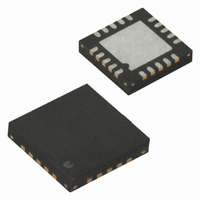
ATTINY13-20MU
Description
IC MCU AVR 1K FLASH 10MHZ 20-MLF
Manufacturer
Atmel
Series
AVR® ATtinyr
Specifications of ATTINY13-20MU
Core Processor
AVR
Core Size
8-Bit
Speed
20MHz
Peripherals
Brown-out Detect/Reset, POR, PWM, WDT
Number Of I /o
6
Program Memory Size
1KB (512 x 16)
Program Memory Type
FLASH
Eeprom Size
64 x 8
Ram Size
64 x 8
Voltage - Supply (vcc/vdd)
2.7 V ~ 5.5 V
Data Converters
A/D 4x10b
Oscillator Type
Internal
Operating Temperature
-40°C ~ 85°C
Package / Case
20-MLF®, QFN
Processor Series
ATTINY1x
Core
AVR8
Data Bus Width
8 bit
Data Ram Size
64 B
Interface Type
SPI
Maximum Clock Frequency
20 MHz
Number Of Programmable I/os
6
Number Of Timers
2
Operating Supply Voltage
2.7 V to 5.5 V
Maximum Operating Temperature
+ 85 C
Mounting Style
SMD/SMT
3rd Party Development Tools
EWAVR, EWAVR-BL
Development Tools By Supplier
ATAVRDRAGON, ATSTK500, ATSTK600, ATAVRISP2, ATAVRONEKIT, ATAKSTK511
Minimum Operating Temperature
- 40 C
On-chip Adc
10 bit, 4 Channel
Package
20MLF EP
Device Core
AVR
Family Name
ATtiny
Maximum Speed
20 MHz
For Use With
ATSTK600-DIP40 - STK600 SOCKET/ADAPTER 40-PDIP770-1007 - ISP 4PORT ATMEL AVR MCU SPI/JTAGATAVRDRAGON - KIT DRAGON 32KB FLASH MEM AVRATAVRISP2 - PROGRAMMER AVR IN SYSTEMATJTAGICE2 - AVR ON-CHIP D-BUG SYSTEM
Lead Free Status / RoHS Status
Lead free / RoHS Compliant
Connectivity
-
Lead Free Status / Rohs Status
Details


16.7
16.8
100
Preventing Flash Corruption
Programming Time for Flash when Using SPM
ATtiny13
To read the Fuse High Byte (FHB), simply replace the address in the Z-pointer with 0x0003 and
repeat the procedure above.
If successful, the contents of the destination register are as follows.
See sections
for more information on fuse and lock bits.
During periods of low V
too low for the CPU and the Flash to operate properly. These issues are the same as for board
level systems using the Flash, and the same design solutions should be applied.
A Flash program corruption can be caused by two situations when the voltage is too low. First, a
regular write sequence to the Flash requires a minimum voltage to operate correctly. Secondly,
the CPU itself can execute instructions incorrectly, if the supply voltage for executing instructions
is too low.
Flash corruption can easily be avoided by following these design recommendations (one is
sufficient):
The calibrated RC Oscillator is used to time Flash accesses.
typical programming time for Flash accesses from the CPU.
Table 16-1.
Note:
Bit
Rd
Flash write (Page Erase, Page Write, and
write lock bits by SPM)
1. Keep the AVR RESET active (low) during periods of insufficient power supply voltage.
2. Keep the AVR core in Power-down sleep mode during periods of low V
This can be done by enabling the internal Brown-out Detector (BOD) if the operating
voltage matches the detection level. If not, an external low V
can be used. If a reset occurs while a write operation is in progress, the write operation
will be completed provided that the power supply voltage is sufficient.
vent the CPU from attempting to decode and execute instructions, effectively protecting
the SPMCSR Register and thus the Flash from unintentional writes.
1. The min and max programming times is per individual operation.
“Program And Data Memory Lock Bits” on page 102
SPM Programming Time
FHB7
Symbol
7
CC
FHB6
, the Flash program can be corrupted because the supply voltage is
6
FHB5
5
(1)
Min Programming Time
FHB4
4
3.7 ms
FHB3
3
Table 16-1 on page 100
FHB2
2
and
CC
reset protection circuit
Max Programming Time
“Fuse Bytes” on page 103
FHB1
1
CC
4.5 ms
. This will pre-
FHB0
0
2535J–AVR–08/10
shows the
Related parts for ATTINY13-20MU
Image
Part Number
Description
Manufacturer
Datasheet
Request
R

Part Number:
Description:
IC MCU AVR 1K FLASH 20MHZ 8SOIC
Manufacturer:
Atmel
Datasheet:

Part Number:
Description:
Manufacturer:
Atmel Corporation
Datasheet:
Part Number:
Description:
IC MCU AVR 1K FLASH 20MHZ 8SOIC
Manufacturer:
Atmel
Datasheet:

Part Number:
Description:
IC MCU AVR 1K FLASH 20MHZ 8DIP
Manufacturer:
Atmel
Datasheet:

Part Number:
Description:
MCU AVR 1KB FLASH 20MHZ 3X3 QFN
Manufacturer:
Atmel
Datasheet:
Part Number:
Description:
IC MCU AVR 1K FLASH 20MHZ 8SOIC
Manufacturer:
Atmel
Datasheet:
Part Number:
Description:
IC MCU AVR 1K 5V 20MHZ 8DIP
Manufacturer:
Atmel
Datasheet:
Part Number:
Description:
IC MCU AVR 1K 5V 20MHZ 8SOIC
Manufacturer:
Atmel
Datasheet:
Part Number:
Description:
IC MCU AVR 1K 5V 20MHZ 8SOIC
Manufacturer:
Atmel
Datasheet:
Part Number:
Description:
IC MCU AVR 1K FLASH 20MHZ 8DIP
Manufacturer:
Atmel
Datasheet:
Part Number:
Description:
IC MCU AVR 1K FLASH 20MHZ 8SOIC
Manufacturer:
Atmel
Datasheet:
Part Number:
Description:
MCU AVR 1KB FLASH 20MHZ 8SOIC GW
Manufacturer:
Atmel
Datasheet: