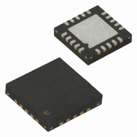
ATTINY13-20MU Atmel, ATTINY13-20MU Datasheet - Page 45

ATTINY13-20MU
Manufacturer Part Number
ATTINY13-20MU
Description
IC MCU AVR 1K FLASH 10MHZ 20-MLF
Manufacturer
Atmel
Series
AVR® ATtinyr
Specifications of ATTINY13-20MU
Core Processor
AVR
Core Size
8-Bit
Speed
20MHz
Peripherals
Brown-out Detect/Reset, POR, PWM, WDT
Number Of I /o
6
Program Memory Size
1KB (512 x 16)
Program Memory Type
FLASH
Eeprom Size
64 x 8
Ram Size
64 x 8
Voltage - Supply (vcc/vdd)
2.7 V ~ 5.5 V
Data Converters
A/D 4x10b
Oscillator Type
Internal
Operating Temperature
-40°C ~ 85°C
Package / Case
20-MLF®, QFN
Processor Series
ATTINY1x
Core
AVR8
Data Bus Width
8 bit
Data Ram Size
64 B
Interface Type
SPI
Maximum Clock Frequency
20 MHz
Number Of Programmable I/os
6
Number Of Timers
2
Operating Supply Voltage
2.7 V to 5.5 V
Maximum Operating Temperature
+ 85 C
Mounting Style
SMD/SMT
3rd Party Development Tools
EWAVR, EWAVR-BL
Development Tools By Supplier
ATAVRDRAGON, ATSTK500, ATSTK600, ATAVRISP2, ATAVRONEKIT, ATAKSTK511
Minimum Operating Temperature
- 40 C
On-chip Adc
10 bit, 4 Channel
Package
20MLF EP
Device Core
AVR
Family Name
ATtiny
Maximum Speed
20 MHz
For Use With
ATSTK600-DIP40 - STK600 SOCKET/ADAPTER 40-PDIP770-1007 - ISP 4PORT ATMEL AVR MCU SPI/JTAGATAVRDRAGON - KIT DRAGON 32KB FLASH MEM AVRATAVRISP2 - PROGRAMMER AVR IN SYSTEMATJTAGICE2 - AVR ON-CHIP D-BUG SYSTEM
Lead Free Status / RoHS Status
Lead free / RoHS Compliant
Connectivity
-
Lead Free Status / Rohs Status
Details
9.2
9.2.1
9.2.2
2535J–AVR–08/10
External Interrupts
Low Level Interrupt
Pin Change Interrupt Timing
The External Interrupts are triggered by the INT0 pin or any of the PCINT5..0 pins. Observe that,
if enabled, the interrupts will trigger even if the INT0 or PCINT5..0 pins are configured as out-
puts. This feature provides a way of generating a software interrupt. Pin change interrupts PCI
will trigger if any enabled PCINT5..0 pin toggles. The PCMSK Register control which pins con-
tribute to the pin change interrupts. Pin change interrupts on PCINT5..0 are detected
asynchronously. This implies that these interrupts can be used for waking the part also from
sleep modes other than Idle mode.
The INT0 interrupts can be triggered by a falling or rising edge or a low level. This is set up as
indicated in the specification for the MCU Control Register – MCUCR. When the INT0 interrupt is
enabled and is configured as level triggered, the interrupt will trigger as long as the pin is held
low. Note that recognition of falling or rising edge interrupts on INT0 requires the presence of an
I/O clock, described in
A low level interrupt on INT0 is detected asynchronously. This implies that this interrupt can be
used for waking the part also from sleep modes other than Idle mode. The I/O clock is halted in
all sleep modes except Idle mode.
Note that if a level triggered interrupt is used for wake-up from Power-down, the required level
must be held long enough for the MCU to complete the wake-up to trigger the level interrupt. If
the level disappears before the end of the Start-up Time, the MCU will still wake up, but no inter-
rupt will be generated. The start-up time is defined by the SUT and CKSEL fuses as described in
“System Clock and Clock Options” on page
If the low level on the interrupt pin is removed before the device has woken up then program
execution will not be diverted to the interrupt service routine but continue from the instruction fol-
lowing the SLEEP command.
An example of timing of a pin change interrupt is shown in
Figure 9-1.
Timing of pin change interrupts
pcint_setflag
pcint_in_(n)
PCINT(n)
pcint_syn
pin_sync
pin_lat
PCINT(0)
“Clock Systems and their Distribution” on page
PCIF
clk
clk
LE
pin_lat
D
Q
pin_sync
PCINT(0) in PCMSK(x)
23.
pcint_in_(0)
0
x
clk
Figure 9-1
pcint_syn
pcint_setflag
below.
23.
PCIF
45


