TOOLSTICK542PP Silicon Laboratories Inc, TOOLSTICK542PP Datasheet - Page 87
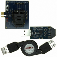
TOOLSTICK542PP
Manufacturer Part Number
TOOLSTICK542PP
Description
PLATFORM PROG TOOLSTICK F542
Manufacturer
Silicon Laboratories Inc
Series
ToolStickr
Type
Microcontroller Programmerr
Specifications of TOOLSTICK542PP
Contents
2 Boards and USB Connecting Cable
Processor To Be Evaluated
C8051F542
Interface Type
USB
Operating Supply Voltage
2.7 V to 3.6 V
Lead Free Status / RoHS Status
Lead free / RoHS Compliant
For Use With/related Products
C8051F542
Lead Free Status / Rohs Status
Lead free / RoHS Compliant
Other names
336-1718


11.2.1.1. General Purpose Registers
The lower 32 bytes of data memory, locations 0x00 through 0x1F, may be addressed as four banks of gen-
eral-purpose registers. Each bank consists of eight byte-wide registers designated R0 through R7. Only
one of these banks may be enabled at a time. Two bits in the program status word, RS0 (PSW.3) and RS1
(PSW.4), select the active register bank (see description of the PSW in SFR Definition 10.6). This allows
fast context switching when entering subroutines and interrupt service routines. Indirect addressing modes
use registers R0 and R1 as index registers.
11.2.1.2. Bit Addressable Locations
In addition to direct access to data memory organized as bytes, the sixteen data memory locations at 0x20
through 0x2F are also accessible as 128 individually addressable bits. Each bit has a bit address from
0x00 to 0x7F. Bit 0 of the byte at 0x20 has bit address 0x00 while bit7 of the byte at 0x20 has bit address
0x07. Bit 7 of the byte at 0x2F has bit address 0x7F. A bit access is distinguished from a full byte access by
the type of instruction used (bit source or destination operands as opposed to a byte source or destina-
tion).
The MCS-51™ assembly language allows an alternate notation for bit addressing of the form XX.B where
XX is the byte address and B is the bit position within the byte. For example, the instruction:
MOV
moves the Boolean value at 0x13 (bit 3 of the byte at location 0x22) into the Carry flag.
11.2.1.3. Stack
A programmer's stack can be located anywhere in the 256-byte data memory. The stack area is desig-
nated using the Stack Pointer (SP) SFR. The SP will point to the last location used. The next value pushed
on the stack is placed at SP+1 and then SP is incremented. A reset initializes the stack pointer to location
0x07. Therefore, the first value pushed on the stack is placed at location 0x08, which is also the first regis-
ter (R0) of register bank 1. Thus, if more than one register bank is to be used, the SP should be initialized
to a location in the data memory not being used for data storage. The stack depth can extend up to
256 bytes.
11.3. External RAM
For C8051F54x devices, 1 kB of RAM are included on-chip and mapped into the external data memory
space (XRAM). The external memory space may be accessed using the external move instruction (MOVX)
and the data pointer (DPTR), or using the MOVX indirect addressing mode using R0 or R1. If the MOVX
instruction is used with an 8-bit address operand (such as @R1), then the high byte of the 16-bit address is
provided by the External Memory Interface Control Register (EMI0CN, shown in SFR Definition 11.1).
Note: The MOVX instruction can also be used for writing to the Flash memory. See Section “
11.3.1. 16-Bit MOVX Example
The 16-bit form of the MOVX instruction accesses the memory location pointed to by the contents of the
DPTR register. The following series of instructions reads the value of the byte at address 0x1234 into the
accumulator A:
The above example uses the 16-bit immediate MOV instruction to set the contents of DPTR. Alternately,
page
C, 22.3h
MOV
MOVX
117
for details. The MOVX instruction accesses XRAM by default.
DPTR, #1234h
A, @DPTR
; load DPTR with 16-bit address to read (0x1234)
; load contents of 0x1234 into accumulator A
Rev. 1.1
C8051F54x
14. Flash Memory
” on
87
Related parts for TOOLSTICK542PP
Image
Part Number
Description
Manufacturer
Datasheet
Request
R

Part Number:
Description:
KIT TOOL EVAL SYS IN A USB STICK
Manufacturer:
Silicon Laboratories Inc
Datasheet:

Part Number:
Description:
TOOLSTICK DEBUG ADAPTER
Manufacturer:
Silicon Laboratories Inc
Datasheet:

Part Number:
Description:
TOOLSTICK BASE ADAPTER
Manufacturer:
Silicon Laboratories Inc
Datasheet:

Part Number:
Description:
TOOLSTICK DAUGHTER CARD
Manufacturer:
Silicon Laboratories Inc
Datasheet:

Part Number:
Description:
TOOLSTICK DAUGHTER CARD
Manufacturer:
Silicon Laboratories Inc
Datasheet:

Part Number:
Description:
TOOLSTICK DAUGHTER CARD
Manufacturer:
Silicon Laboratories Inc
Datasheet:

Part Number:
Description:
TOOLSTICK DAUGHTER CARD
Manufacturer:
Silicon Laboratories Inc
Datasheet:

Part Number:
Description:
KIT STARTER TOOLSTICK
Manufacturer:
Silicon Laboratories Inc
Datasheet:

Part Number:
Description:
KIT UNIVERSITY TOOLSTICK STARTER
Manufacturer:
Silicon Laboratories Inc
Datasheet:

Part Number:
Description:
DAUGHTER CARD TOOLSTICK F330
Manufacturer:
Silicon Laboratories Inc
Datasheet:

Part Number:
Description:
CARD DAUGHTER UNIVRSTY TOOLSTICK
Manufacturer:
Silicon Laboratories Inc
Datasheet:

Part Number:
Description:
DAUGHTER CARD TOOLSTICK F582
Manufacturer:
Silicon Laboratories Inc
Datasheet:

Part Number:
Description:
DAUGHTER CARD TOOLSTICK F500
Manufacturer:
Silicon Laboratories Inc
Datasheet:

Part Number:
Description:
DAUGHTER CARD TOOLSTICK F540
Manufacturer:
Silicon Laboratories Inc
Datasheet:

Part Number:
Description:
DAUGHTER CARD TOOLSTICK F560
Manufacturer:
Silicon Laboratories Inc
Datasheet: