TOOLSTICK542PP Silicon Laboratories Inc, TOOLSTICK542PP Datasheet - Page 6
TOOLSTICK542PP
Manufacturer Part Number
TOOLSTICK542PP
Description
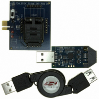
PLATFORM PROG TOOLSTICK F542
Manufacturer
Silicon Laboratories Inc
Series
ToolStickr
Type
Microcontroller Programmerr
Specifications of TOOLSTICK542PP
Contents
2 Boards and USB Connecting Cable
Processor To Be Evaluated
C8051F542
Interface Type
USB
Operating Supply Voltage
2.7 V to 3.6 V
Lead Free Status / RoHS Status
Lead free / RoHS Compliant
For Use With/related Products
C8051F542
Lead Free Status / Rohs Status
Lead free / RoHS Compliant
Other names
336-1718


C8051F54x
List of Figures
6
Figure 1.1. C8051F540/1/4/5 Block Diagram .......................................................... 14
Figure 1.2. C8051F542/3/6/7 Block Diagram .......................................................... 15
Figure 3.1. QFP-32 Pinout Diagram (Top View) ...................................................... 20
Figure 3.2. QFN-32 Pinout Diagram (Top View) ..................................................... 21
Figure 3.3. QFN-24 Pinout Diagram (Top View) ..................................................... 22
Figure 4.1. QFP-32 Package Drawing ..................................................................... 23
Figure 4.2. QFP-32 Landing Diagram ..................................................................... 24
Figure 4.3. QFN-32 Package Drawing .................................................................... 25
Figure 4.4. QFN-32 Landing Diagram ..................................................................... 26
Figure 4.5. QFN-24 Package Drawing .................................................................... 27
Figure 4.6. QFN-24 Landing Diagram ..................................................................... 28
Figure 5.1. ADC0 Functional Block Diagram ........................................................... 29
Figure 5.2. ADC0 Tracking Modes .......................................................................... 31
Figure 5.3. 12-Bit ADC Tracking Mode Example ..................................................... 32
Figure 5.4. 12-Bit ADC Burst Mode Example With Repeat Count Set to 4 ............. 33
Figure 5.5. ADC0 Equivalent Input Circuit ............................................................... 35
Figure 5.6. ADC Window Compare Example: Right-Justified Data ......................... 46
Figure 5.7. ADC Window Compare Example: Left-Justified Data ........................... 46
Figure 6.1. Minimum VDD Monitor Threshold vs. System Clock Frequency ........... 50
Figure 6.2. ADC0 Multiplexer Block Diagram .......................................................... 58
Figure 6.3. Temperature Sensor Transfer Function ................................................ 60
Figure 7.1. Voltage Reference Functional Block Diagram ....................................... 61
Figure 8.1. Comparator Functional Block Diagram ................................................. 63
Figure 8.2. Comparator Hysteresis Plot .................................................................. 64
Figure 8.3. Comparator Input Multiplexer Block Diagram ........................................ 69
Figure 9.1. External Capacitors for Voltage Regulator Input/Output—
Figure 9.2. External Capacitors for Voltage Regulator Input/Output—Regulator Dis-
Figure 10.1. CIP-51 Block Diagram ......................................................................... 75
Figure 11.1. C8051F54x Memory Map .................................................................... 85
Figure 11.2. Flash Program Memory Map ............................................................... 86
Figure 12.1. SFR Page Stack .................................................................................. 90
Figure 12.2. SFR Page Stack While Using SFR Page 0x0 To Access SMB0ADR . 91
Figure 12.3. SFR Page Stack After SPI0 Interrupt Occurs ...................................... 92
Figure 12.4. SFR Page Stack Upon PCA Interrupt Occurring During a SPI0 ISR .. 93
Figure 12.5. SFR Page Stack Upon Return From PCA Interrupt ............................ 94
Figure 12.6. SFR Page Stack Upon Return From SPI0 Interrupt ............................ 95
Figure 14.1. Flash Program Memory Map ............................................................. 119
Figure 16.1. Reset Sources ................................................................................... 129
Figure 16.2. Power-On and VDD Monitor Reset Timing ....................................... 130
Figure 17.1. Oscillator Options .............................................................................. 135
Figure 17.2. Example Clock Multiplier Output ....................................................... 140
Regulator Enabled ............................................................................................. 72
abled
............................................................................................................... 73
Rev. 1.1
Related parts for TOOLSTICK542PP
Image
Part Number
Description
Manufacturer
Datasheet
Request
R

Part Number:
Description:
KIT TOOL EVAL SYS IN A USB STICK
Manufacturer:
Silicon Laboratories Inc
Datasheet:

Part Number:
Description:
TOOLSTICK DEBUG ADAPTER
Manufacturer:
Silicon Laboratories Inc
Datasheet:

Part Number:
Description:
TOOLSTICK BASE ADAPTER
Manufacturer:
Silicon Laboratories Inc
Datasheet:

Part Number:
Description:
TOOLSTICK DAUGHTER CARD
Manufacturer:
Silicon Laboratories Inc
Datasheet:

Part Number:
Description:
TOOLSTICK DAUGHTER CARD
Manufacturer:
Silicon Laboratories Inc
Datasheet:

Part Number:
Description:
TOOLSTICK DAUGHTER CARD
Manufacturer:
Silicon Laboratories Inc
Datasheet:

Part Number:
Description:
TOOLSTICK DAUGHTER CARD
Manufacturer:
Silicon Laboratories Inc
Datasheet:

Part Number:
Description:
KIT STARTER TOOLSTICK
Manufacturer:
Silicon Laboratories Inc
Datasheet:

Part Number:
Description:
KIT UNIVERSITY TOOLSTICK STARTER
Manufacturer:
Silicon Laboratories Inc
Datasheet:

Part Number:
Description:
DAUGHTER CARD TOOLSTICK F330
Manufacturer:
Silicon Laboratories Inc
Datasheet:

Part Number:
Description:
CARD DAUGHTER UNIVRSTY TOOLSTICK
Manufacturer:
Silicon Laboratories Inc
Datasheet:

Part Number:
Description:
DAUGHTER CARD TOOLSTICK F582
Manufacturer:
Silicon Laboratories Inc
Datasheet:

Part Number:
Description:
DAUGHTER CARD TOOLSTICK F500
Manufacturer:
Silicon Laboratories Inc
Datasheet:

Part Number:
Description:
DAUGHTER CARD TOOLSTICK F540
Manufacturer:
Silicon Laboratories Inc
Datasheet:

Part Number:
Description:
DAUGHTER CARD TOOLSTICK F560
Manufacturer:
Silicon Laboratories Inc
Datasheet: