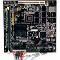
MPC8349E-MITX-GP Freescale Semiconductor, MPC8349E-MITX-GP Datasheet - Page 7

MPC8349E-MITX-GP
Manufacturer Part Number
MPC8349E-MITX-GP
Description
KIT REFERENCE PLATFORM MPC8349E
Manufacturer
Freescale Semiconductor
Series
PowerQUICC II™ PROr
Type
MPUr
Datasheets
1.MPC8349E-MITX-GP.pdf
(36 pages)
2.MPC8349E-MITX-GP.pdf
(2 pages)
3.MPC8349E-MITX-GP.pdf
(1 pages)
Specifications of MPC8349E-MITX-GP
Contents
Module and Misc Hardware
For Use With/related Products
MPC8349E
Lead Free Status / RoHS Status
Lead free / RoHS Compliant
1.2.4
MPC8349E uses DDR SDRAM as the system memory. The DDR interface uses the SSTL2 driver/receiver
and 2.5 V power. A Vref 2.5V/2 is needed for all SSTL2 receivers in the DDR interface. For details on
DDR timing design and termination, refer to the Freescale application note entitled Hardware and Layout
Design Considerations for DDR Memory Interfaces (AN2582). The termination scheme uses one series
resistor (R
termination rail (V
The MPC8349E reads the DIMM SPD data using the DIMM SCL (clock) and the SDA (data) signals
through the I2C2 interface.
Freescale Semiconductor
66.666 MHz
125 MHz
133/166 MHz
25 MHz
33/66 MHz
24 MHz
32.768 KHz
Clock Frequency
S
) from the MPC8349E to the memory and one termination resistor (R
DDR SDRAM Controller
MPC8349E CLKIN
MPC8349E TSEC
DDR SDRAM
GBE PHY (VSC8201)
PCI 32-bit slot
USB PHY2 (USB3300)
RTC (DS1339)
TT
). This approach is used in commodity PC motherboard designs.
MPC8349E-mITX-GP Reference Design Platform User’s Guide, Rev. 0
Module
Figure 5
Preliminary—Subject to Change Without Notice
shows the DDR SDRAM controller connection.
Table 1. Clock Distribution
66.666 MHz oscillator
VSC8201
MPC8349E
125 MHz oscillator
MPC8349E
24 MHz crystal
32.768 KHz crystal
Generated by
The MPC834x uses CLKIN to generate the
PCI_SYNC_OUT clock signal, which is fed back
on the board through the PCI_SYNC_IN signal
to the internal system PLL. From the power-on
reset configuration, the CSB clock is generated
by the internal PLL and is fed to the e300 core
PLL for generating the e300 core clock. The
GPL5 (CFG_CLKIN_DIV) configuration input
selects whether CLKIN or CLKIN/2 is driven on
the PCI_SYNC_OUT signal. The GPL5 is tied to
jumper J22.D.
For TSEC operation, a 125 MHz clock is
provided by the gigabit Ethernet PHY
(VSC8201) on the board.
The DDR memory controller is configured to use
the 1:1 mode CSB to DDR clock for the DDR
interface. The local bus clock uses CCB/n clock,
where n is configured from the LCRR register.
The 25 MHz oscillator generates the clock for
the VSC8201
The PCI module uses the PCI_SYNC_IN as its
clock source. The trace of the PCI_SYNC_IN/
PCI_SYNC_OUT signal is synchronized with all
the PCI signals of the PCI slots. The trace length
of the PCI_SYNC_IN/PCI_SYNC_OUT clock is
2.5 inches from the pin of the PowerQUICC II
Pro device to the PCI sockets.
Description
T
) attached to the
MPC8349E-mITX-GP Board
7


