MPC8349E-MITX-GP Freescale Semiconductor, MPC8349E-MITX-GP Datasheet - Page 18
MPC8349E-MITX-GP
Manufacturer Part Number
MPC8349E-MITX-GP
Description
KIT REFERENCE PLATFORM MPC8349E
Manufacturer
Freescale Semiconductor
Series
PowerQUICC II™ PROr
Type
MPUr
Datasheets
1.MPC8349E-MITX-GP.pdf
(36 pages)
2.MPC8349E-MITX-GP.pdf
(2 pages)
3.MPC8349E-MITX-GP.pdf
(1 pages)
Specifications of MPC8349E-MITX-GP
Contents
Module and Misc Hardware
For Use With/related Products
MPC8349E
Lead Free Status / RoHS Status
Lead free / RoHS Compliant


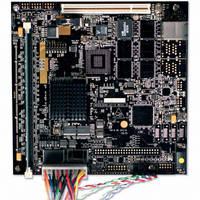
MPC8349E-mITX-GP Board
1.5
This section shows the default settings and descriptions of jumpers, switches, and LED indicators.
1.5.1
The powerup configuration jumpers at J22 sets up the system configurations.
default configuration of J22.
Table 8
18
Position
C
D
A
B
E
describes the position of each jumper.
Jumpers, Switches, and LED Indicators
BOOT1
LGPL0
LGPL1
LGPL3
LGPL5
Powerup Configuration Jumpers
Name
Jumper On
OFF = Jumper Is Off
MPC8349E-mITX-GP Reference Design Platform User’s Guide, Rev. 0
ON = Jumper Is On
OFF (1)
Default
ON (0)
ON (0)
ON (0)
OFF(1)
Figure 16. Powerup Configuration Jumpers (J22)
A
Table 8. Description of Jumper J22 Positions
Preliminary—Subject to Change Without Notice
B
000 local bus EEPROM (Default)
001 I
010 I
011 Hard-coded option, 66 MHz, 266 MHz, 400 MHz (PCI, CSB, CPU)
100 Hard-coded option, 33 MHz, 266 MHz, 400 MHz
101 Hard-coded option, 33 MHz, 133 MHz, 266 MHz
110 Hard-coded option, 33 MHz, 166 MHz, 333 MHz
111 Hard-coded option, 66 MHz, 266 MHz, 533 MHz
Hard-coded option is used in conjunction with JTAG debug
OFF (1): Default
CLKIN: PCI_SYNC_OUT = 2:1 PCI_CLK_OUT[0:7] = OCCR (max CLKIN/2).
66 MHz CLKIN is used and 33 MHz PCI2.
ON (0):
CLKIN: PCI_SYNC_OUT = 1:1, PCI_CLK_OUT[0:7] = CLKIN. 66 MHz
CLKIN is used, 66 MHz PCI2.
OFF (1): Default
MPC8349E fetches the reset vector from Flash 0 (U4).
ON (0): Reserved
C
2
2
C EEPROM,PCI_CLK/PCI_SYNC_IN 25–44 MHz
C EEPROM,PCI_CLK/PCI_SYNC_IN 25–66.666 MHz
D
E
F
G
Description
H
Jumper Off
Figure 16
Freescale Semiconductor
shows the factory
Related parts for MPC8349E-MITX-GP
Image
Part Number
Description
Manufacturer
Datasheet
Request
R

Part Number:
Description:
BOARD REFERENCE FOR MPC8349
Manufacturer:
Freescale Semiconductor
Datasheet:

Part Number:
Description:
KIT MODULAR DEV SYSTEM MPC8349E
Manufacturer:
Freescale Semiconductor
Datasheet:

Part Number:
Description:
MCU, MPU & DSP Development Tools PROCESSR BD MPC8349E
Manufacturer:
Freescale Semiconductor
Part Number:
Description:
MCU, MPU & DSP Development Tools KIT FOR MPC8349E BDS
Manufacturer:
Freescale Semiconductor

Part Number:
Description:
Manufacturer:
Freescale Semiconductor, Inc
Datasheet:
Part Number:
Description:
Manufacturer:
Freescale Semiconductor, Inc
Datasheet:
Part Number:
Description:
Manufacturer:
Freescale Semiconductor, Inc
Datasheet:
Part Number:
Description:
Manufacturer:
Freescale Semiconductor, Inc
Datasheet:
Part Number:
Description:
Manufacturer:
Freescale Semiconductor, Inc
Datasheet:
Part Number:
Description:
Manufacturer:
Freescale Semiconductor, Inc
Datasheet:
Part Number:
Description:
Manufacturer:
Freescale Semiconductor, Inc
Datasheet:
Part Number:
Description:
Manufacturer:
Freescale Semiconductor, Inc
Datasheet:
Part Number:
Description:
Manufacturer:
Freescale Semiconductor, Inc
Datasheet:
Part Number:
Description:
Manufacturer:
Freescale Semiconductor, Inc
Datasheet:
Part Number:
Description:
Manufacturer:
Freescale Semiconductor, Inc
Datasheet: