HSC-ADC-EVALCZ Analog Devices Inc, HSC-ADC-EVALCZ Datasheet - Page 10
HSC-ADC-EVALCZ
Manufacturer Part Number
HSC-ADC-EVALCZ
Description
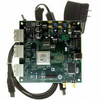
KIT EVAL ADC FIFO HI SPEED
Manufacturer
Analog Devices Inc
Datasheets
1.HSC-ADC-EVALB-DCZ.pdf
(28 pages)
2.HSC-ADC-EVALCZ.pdf
(32 pages)
3.HSC-ADC-EVALCZ.pdf
(40 pages)
Specifications of HSC-ADC-EVALCZ
Design Resources
EVALC PC Board Gerber File
Accessory Type
ADC Interface Board
Silicon Manufacturer
Analog Devices
Application Sub Type
ADC
Kit Application Type
Data Converter
Features
Buffer Memory Board For Capturing Digital Data, USB Port Interface, Windows 98, Windows 2000
Kit Contents
ADC Analyzer, Buffer Memory Board
Rohs Compliant
Yes
Lead Free Status / RoHS Status
Lead free / RoHS Compliant
For Use With/related Products
Single ADC Version
Lead Free Status / Rohs Status
Supplier Unconfirmed
Available stocks
Company
Part Number
Manufacturer
Quantity
Price
Company:

Part Number:
HSC-ADC-EVALCZ
Manufacturer:
Analog Devices Inc
Quantity:
135


HSC-ADC-EVALB-SC/HSC-ADC-EVALB-DC
The SPI interface designed on the Cypress IC can communicate
with up to five different SPI-enabled devices. The CLK and data
lines are common to all SPI devices. The correct device is
chosen to communicate by using one of the five active low chip
select pins. This functionality is controlled by selecting a SPI
channel in the software.
CLOCKING WITH INTERLEAVED DATA
ADCs with very high data rates can exceed the capability of a
single buffer memory channel (~133 MSPS). These converters
often demultiplex the data into two channels to reduce the rate
required to capture the data. In these applications, ADC Analyzer
must interleave the data from both channels to process it as a
single channel. The user can configure the software to process
the first sample from Channel A, the second from Channel B,
and so on, or vice versa. The synchronization circuit included in
the buffer memory forces a small delay between the write enable
signals (WENA and WENB) to the FIFO memory chips (Pin 1,
U101, and U201), ensuring that the data is captured in one
FIFO before the other. Jumper J401 and Jumper J402 determine
which FIFO receives WENA and which FIFO receives WENB.
CONNECTING TO THE HSC-ADC-FPGA-4/-8
ADCs that have serial LVDS outputs require another board that
is connected between the ADC evaluation board and the FIFO
data capture card. This board converts the serial data into
parallel CMOS so that the FIFO data capture card can accept
the data. For more detailed information on this board, refer to
the HSC-ADC-FPGA datasheet at www.analog.com/hsc-FIFO.
Rev. 0 | Page 10 of 28
CONNECTING TO THE DEMUX BRD
ADCs that have parallel LVDS outputs require another board
that is connected between the ADC evaluation board and the
FIFO data capture card. This board converts parallel LVDS to
parallel CMOS, using both channels of the FIFO data capture
card. For more detailed information on this board, send an
email to
UPGRADING FIFO MEMORY
The FIFO evaluation board includes one or two 32 kB FIFOs
that are capable of 133 MHz clock signals, depending on the
model number. Pin-compatible FIFO upgrades are available
from IDT. See Table 2 for the IDT part number matrix.
Table 2. IDT Part Number Matrix
Part Number
IDT72V283-L7-5PF (Default )
IDT72V293-L7-5PF
IDT72V2103-L7-5PF
IDT72V2113-L7-5PF
IDT72V283-L6PF
IDT72V293-L6PF
IDT72V2103-L6PF
IDT72V2113-L6PF
For more information, visit www.idt.com.
highspeed.converters@analog.com
FIFO Depth
32 kB
64 kB
132 kB
256 kB
32 kB
64 kB
132 kB
256 kB
FIFO Speed
133 MHz
133 MHz
133 MHz
133 MHz
166 MHz
166 MHz
166 MHz
166 MHz
Related parts for HSC-ADC-EVALCZ
Image
Part Number
Description
Manufacturer
Datasheet
Request
R

Part Number:
Description:
KIT EVAL ADC FIFO DUAL-CH USB HS
Manufacturer:
Analog Devices Inc
Datasheet:

Part Number:
Description:
KIT EVAL ADC USB FIFO HI-SPEED
Manufacturer:
Analog Devices Inc
Datasheet:

Part Number:
Description:
BOARD FPGA OCTAL LVDS FOR ADC
Manufacturer:
Analog Devices Inc
Datasheet:
Part Number:
Description:
KIT EVAL FOR SINGLE CHAN HSC ADC
Manufacturer:
Analog Devices Inc

Part Number:
Description:
KIT EVAL FOR DUAL ADC/CONV
Manufacturer:
Analog Devices Inc
Datasheet:
Part Number:
Description:
KIT EVAL ADC USB FIFO HI-SPEED
Manufacturer:
Analog Devices Inc
Datasheet:

Part Number:
Description:
KIT EVAL ADC USB FIFO HI-SPEED
Manufacturer:
Analog Devices Inc
Datasheet:
Part Number:
Description:
KIT EVAL ADC FIFO DUAL-CH USB HS
Manufacturer:
Analog Devices Inc
Datasheet:
Part Number:
Description:
BOARD FPGA QUAD LVDS FOR ADC
Manufacturer:
Analog Devices Inc
Datasheet:
Part Number:
Description:
Adapter For AD922x Family
Manufacturer:
Analog Devices Inc
Datasheet:
Part Number:
Description:
Interposer Quad/octal ADCs
Manufacturer:
Analog Devices Inc
Datasheet:

Part Number:
Description:
±1.7g Dual-Axis IMEMS Accelerometer Evaluation Board
Manufacturer:
Analog Devices Inc
Datasheet:

Part Number:
Description:
IC MULTIPLIER ANALOG 8-SOIC T/R
Manufacturer:
Analog Devices Inc
Datasheet:
Part Number:
Description:
IC ANALOG MULTIPLIER 8-DIP
Manufacturer:
Analog Devices Inc
Datasheet: