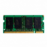
MT4VDDT3264HY-335F2 Micron Technology Inc, MT4VDDT3264HY-335F2 Datasheet - Page 14

MT4VDDT3264HY-335F2
Manufacturer Part Number
MT4VDDT3264HY-335F2
Description
MODULE DDR 256MB 200-SODIMM
Manufacturer
Micron Technology Inc
Specifications of MT4VDDT3264HY-335F2
Memory Type
DDR SDRAM
Memory Size
256MB
Speed
333MT/s
Package / Case
200-SODIMM
Main Category
DRAM Module
Sub-category
DDR SDRAM
Module Type
200SODIMM
Device Core Size
64b
Organization
32Mx64
Total Density
256MByte
Chip Density
512Mb
Access Time (max)
700ps
Maximum Clock Rate
333MHz
Operating Supply Voltage (typ)
2.5V
Operating Current
780mA
Number Of Elements
4
Operating Supply Voltage (max)
2.7V
Operating Supply Voltage (min)
2.3V
Operating Temp Range
0C to 70C
Operating Temperature Classification
Commercial
Pin Count
200
Mounting
Socket
Lead Free Status / RoHS Status
Lead free / RoHS Compliant
Other names
557-1231
MT4VDDT3264HY-335F2
MT4VDDT3264HY-335F2
Table 12: I
DDR SDRAM component values only
Notes: 1–5, 8, 10, 14, 48; notes appear on pages 19–22; 0°C
pdf: 09005aef8086ea3d, source: 09005aef8086ea0b
DD4C8_16_32x64HG.fm - Rev. C 9/04 EN
PARAMETER/CONDITION
OPERATING CURRENT: One device bank; Active-Precharge;
t
once per clock cyle; Address and control inputs changing once
every two clock cycles
OPERATING CURRENT: One device bank; Active -Read Precharge;
Burst = 2;
control inputs changing once per clock cycle
PRECHARGE POWER-DOWN STANDBY CURRENT: All device banks
idle; Power-down mode;
IDLE STANDBY CURRENT: CS# = HIGH; All device banks idle;
t
once per clock cycle. V
ACTIVE POWER-DOWN STANDBY CURRENT: One device bank
active; Power-down mode;
ACTIVE STANDBY CURRENT: CS# = HIGH; CKE = HIGH; One device
bank; Active-Precharge;
andDQS inputs changing twice per clock cycle; Address and other
control inputs changing once per clock cycle
OPERATING CURRENT: Burst = 2; Reads; Continuous burst; One
device bank active; Address and control inputs changing once per
clock cycle;
OPERATING CURRENT: Burst = 2; Writes; Continuous burst; One
device bank active; Address and control inputs changing once per
clock cycle;
twice per clock cycle
AUTO REFRESH CURRENT
SELF REFRESH CURRENT: CKE
OPERATING CURRENT: Four device bank interleaving READs (BL = 4)
with auto precharge,
control inputs change only during Active READ or WRITE
commands
RC =
CK MIN; CKE = HIGH; Address and other control inputs changing
t
RC (MIN);
t
RC =
t
t
CK =
CK =
t
RC (MIN);
t
DD
CK =
t
t
CK (MIN); I
CK (MIN); DQ, DM, and DQS inputs changing
Specifications and Conditions – 64MB
IN
t
t
RC =
CK (MIN); DQ, DM and DQS inputs changing
= V
t
RC =
t
t
CK =
CK =
REF
t
t
CK =
RC (MIN);
OUT
t
for DQ, DQS, and DM
RAS (MAX);
t
0.2V
t
CK (MIN); CKE = (LOW)
CK (MIN); I
= 0mA
t
CK (MIN); CKE = LOW
t
CK =
t
OUT
CK =
t
CK (MIN); Address and
= 0mA; Address and
t
t
t
REFC =
REFC = 15.625µs
CK (MIN); DQ, DM
t
RFC (MIN)
t
14
T
CK =
A
+70°C; V
64MB, 128MB, 256MB (x64, SR)
200-PIN DDR SDRAM SODIMM
I
I
I
I
I
I
I
SYM
DD4W
I
I
DD3N
I
DD5A
I
I
Micron Technology, Inc., reserves the right to change products or specifications without notice.
DD2P
DD3P
DD4R
DD2F
DD0
DD1
DD5
DD6
DD7
DD
= V
1,060
1,540
-335
DD
500
540
180
100
200
580
620
12
20
12
Q = +2.5V ±0.2V
MAX
1,000
1,500
-262
460
540
180
100
200
560
540
12
20
12
©2004 Micron Technology, Inc. All rights reserved.
-26A/
1,000
1,500
-265
440
500
160
180
540
520
12
80
20
8
UNITS NOTES
mA
mA
mA
mA
mA
mA
mA
mA
mA
mA
mA
mA
21, 28,
21, 28,
20, 42
20, 42
20, 42
24, 44
20, 43
44
45
44
20
20
44
9


