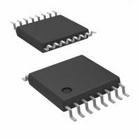
LM5115MTC/NOPB National Semiconductor, LM5115MTC/NOPB Datasheet - Page 6

LM5115MTC/NOPB
Manufacturer Part Number
LM5115MTC/NOPB
Description
IC CTRLR SSPR MULT OUTPT 16TSSOP
Manufacturer
National Semiconductor
Type
Step-Down (Buck)r
Datasheet
1.LM5115SDNOPB.pdf
(17 pages)
Specifications of LM5115MTC/NOPB
Internal Switch(s)
No
Synchronous Rectifier
Yes
Number Of Outputs
2
Voltage - Output
0.7 ~ 13.5 V
Current - Output
20A
Frequency - Switching
1MHz
Voltage - Input
4.5 ~ 75 V
Operating Temperature
-40°C ~ 125°C
Mounting Type
Surface Mount
Package / Case
16-TSSOP
Power - Output
300W
For Use With
LM5115EVAL - BOARD EVALUATION LM5115LM5115DC EVAL - BOARD EVALUATION LM5115DCLM5115AEVAL - BOARD EVALUATION LM5115A
Lead Free Status / RoHS Status
Lead free / RoHS Compliant
Other names
*LM5115MTC
*LM5115MTC/NOPB
LM5115MTC
*LM5115MTC/NOPB
LM5115MTC
Available stocks
Company
Part Number
Manufacturer
Quantity
Price
Part Number:
LM5115MTC/NOPB
Manufacturer:
NS/国半
Quantity:
20 000
www.national.com
CURRENT LIMIT
RAMP GENERATOR
LOW SIDE GATE DRIVER
HIGH SIDE GATE DRIVER
SWITCHING CHARACTERISITCS
THERMAL SHUTDOWN
THERMAL RESISTANCE
SYMBOL
Electrical Characteristics
or HO. (Continued)
VCLneg
Note 1: Absolute Maximum Ratings indicate limits beyond which damage to the component may occur. Operating Ratings are conditions under which operation of
the device is guaranteed. Operating Ratings do not imply guaranteed performance limits. For guaranteed performance limits and associated test conditions, see the
Electrical Characteristics tables.
Note 2: The human body model is a 100 pF capacitor discharged through a 1.5k
Note 3: Min and Max limits are 100% production tested at 25˚C. Limits over the operating temperature range are guaranteed through correlation using Statistical
Quality Control (SQC) methods. Limits are used to calculate National’s Average Outgoing Quality Level (AOQL).
Note 4: Device thermal limitations may limit usable range.
V
V
V
V
I
I
I
I
T
OHH
OHL
OLH
OLL
OHH
OLL
OHL
OLH
SD
JA
JA
ILIMIT Amp Transconductance
Overall Transconductance
Positive Current Limit
Positive Current Limit Foldback
Negative Current Limit
SYNC Input Impedance
SYNC Threshold
Free Run Mode Peak Threshold
Current Mirror Gain
Discharge Impedance
LO Low-state Output Voltage
LO High-state Output Voltage
LO Rise Time
LO Fall Time
Peak LO Source Current
Peak LO Sink Current
HO Low-state Output Voltage
HO High-state Output Voltage
HO Rise Time
HO High Side Fall Time
Peak HO Source Current
Peak HO Sink Current
LO Fall to HO Rise Delay
HO Fall to LO Rise Delay
SYNC Fall to HO Fall Delay
SYNC Rise to LO Fall Delay
Thermal Shutdown Temp.
Thermal Shutdown Hysteresis
Junction to Ambient
Junction to Ambient
PARAMETER
Unless otherwise specified, T
V
VOUT = 6V and CO/COMP = 1.5V
V
VOUT = 0V and CO/COMP = 1.5V
VOUT = 6V
V
shutoff
End of cycle detection threshold
RAMP peak voltage with dc current
applied to SYNC.
Ratio of RAMP charge current to
SYNC input current.
I
I
C
C
V
V
I
I
C
C
V
V
C
C
C
C
MTC Package
SDA Package
LO
LO
HO
HO
CL
CL
CL
LO
LO
HO
HO
LOAD
LOAD
LOAD
LOAD
LOAD
LOAD
LOAD
LOAD
= 100mA
= -100mA, V
= 100mA
= -100mA, V
= V
= V
= V
= 0V
= 12V
= 0V
= 12V
= 1000pF
= 1000pF
= 1000pF
= 1000pF
= 0
= 0
= 0
= 0
CS
CS
CS
- V
- V
- V
CONDITIONS
6
VOUT
VOUT
VOUT
OHL
resistor into each pin.
OHH
to cause LO to
= V
= V
J
= –40˚C to +125˚C, VBIAS = 12V, No Load on LO
CC
HB
-V
–V
LO
HO
MIN
150
2.7
37
31
TYP
237
100
120
165
125
-17
2.5
0.2
0.4
2.5
0.2
0.4
2.5
16
45
38
15
15
12
15
12
70
50
50
25
32
2
2
MAX
2.3
3.3
0.5
0.8
0.5
0.8
53
45
mA / V
mA / V
UNITS
˚C/W
˚C/W
mV
mV
mV
A/A
k
µA
ns
ns
ns
ns
ns
ns
ns
ns
˚C
˚C
V
V
V
A
A
V
V
A
A


