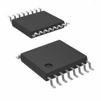
LM5115MTC/NOPB National Semiconductor, LM5115MTC/NOPB Datasheet - Page 10

LM5115MTC/NOPB
Manufacturer Part Number
LM5115MTC/NOPB
Description
IC CTRLR SSPR MULT OUTPT 16TSSOP
Manufacturer
National Semiconductor
Type
Step-Down (Buck)r
Datasheet
1.LM5115SDNOPB.pdf
(17 pages)
Specifications of LM5115MTC/NOPB
Internal Switch(s)
No
Synchronous Rectifier
Yes
Number Of Outputs
2
Voltage - Output
0.7 ~ 13.5 V
Current - Output
20A
Frequency - Switching
1MHz
Voltage - Input
4.5 ~ 75 V
Operating Temperature
-40°C ~ 125°C
Mounting Type
Surface Mount
Package / Case
16-TSSOP
Power - Output
300W
For Use With
LM5115EVAL - BOARD EVALUATION LM5115LM5115DC EVAL - BOARD EVALUATION LM5115DCLM5115AEVAL - BOARD EVALUATION LM5115A
Lead Free Status / RoHS Status
Lead free / RoHS Compliant
Other names
*LM5115MTC
*LM5115MTC/NOPB
LM5115MTC
*LM5115MTC/NOPB
LM5115MTC
Available stocks
Company
Part Number
Manufacturer
Quantity
Price
Part Number:
LM5115MTC/NOPB
Manufacturer:
NS/国半
Quantity:
20 000
www.national.com
Synchronization (SYNC) and
Feed-Forward (RAMP)
lation is improved because the PWM duty cycle of the aux-
iliary converter is immediately corrected, independent of the
delays of the voltage regulation loop.
The recommended SYNC input current range is 50µA to
150µA. The SYNC pin resistor (R
set the SYNC current (I
phase signal amplitude, V
that I
change in phase signal amplitude. The SYNC pin resistor is
therefore:
Once I
RAMP signal amplitude may be programmed by selecting
the proper RAMP pin capacitor value. The recommended
peak amplitude of the RAMP waveform is 1V to 1.75V. The
C
amplitude with the nominal phase signal voltage and pulse
width.
Where
C
I
T
V
For example,
Main channel output = 3.3V. Phase signal maximum ampli-
tude = 12V. Phase signal frequency = 250kHz
• Set I
• T
• Assume desired V
• C
• C
SYNC
ON
RAMP
RAMP
RAMP
tude (12V):
I
(R
R
(3.3V/12V) / 250kHz = 1.1µs
/ 1.5V
SYNC
= corresponding phase signal pulse width
ON
SYNC
RAMP
RAMP
SYNC
SYNC
= SYNC pin current current
SYNC
= RAMP pin capacitance
= desired RAMP amplitude (1V to 1.75V)
capacitor is chosen to provide the desired RAMP
SYNC
= Main channel duty cycle / Phase frequency =
= 150µA = V
R
= 12V/150µA - 2.5k
= (3 x I
= 330pF
stays within the recommended range over a 3:1
+ 2.5 k )
C
SYNC
has been established by selecting R
RAMP
= 150µA with phase signal at maximum ampli-
= (V
SYNC
= (3 x I
PHASE(max)
RAMP
PHASE(max)
x T
SYNC
ON
SYNC
PHASE(max)
= 1.5V
) / V
) to 150µA with the maximum
x T
SYNC
= 77.5k
/ 150µA) - 2.5k
RAMP
/ (R
ON
SYNC
) should be selected to
. This will guarantee
) / V
= (3 x 150µA x 1.1µs)
(Continued)
FIGURE 3. Line Feed-forward Waveforms
+ 2.5 k ) = 12V /
RAMP
SYNC
, the
10
Error Amplifier and Soft-Start (FB,
CO, & COMP, SS)
An internal wide bandwidth error amplifier is provided within
the LM5115 for voltage feedback to the PWM controller. The
amplifier’s inverting input is connected to the FB pin. The
output of the auxiliary converter is regulated by connecting a
voltage setting resistor divider between the output and the
FB pin. Loop compensation networks are connected be-
tween the FB pin and the error amplifier output (COMP). The
amplifier’s non-inverting input is internally connected to the
SS pin. The SS pin is biased at 0.75V by a resistor divider
connected to the internal 1.27V bandgap reference. When
the VCC voltage is below the UVLO threshold, the SS pin is
discharged to ground. When VCC rises and exceeds the
positive going UVLO threshold (4.25V), the SS pin is re-
leased and allowed to rise. If an external capacitor is con-
nected to the SS pin, it will be charged by the internal resistor
divider to gradually increase the non-inverting input of the
error amplifier to 0.75V. The equivalent impedance of the SS
resistor divider is nominally 60k
charging time constant of the SS capacitor. During start-up,
the output of the LM5115 converter will follow the exponen-
tial equation:
Where
Rss = internal resistance of SS pin (60k )
Css = external Soft-Start capacitor
VOUT(final) = regulator output set point
The initial v / t of the output voltage is VOUT(final) / Rss x
Css and VOUT will be within 1% of the final regulation level
after 4.6 time constants or when t = 4.6 x Rss x Css.
Pull-up current for the error amplifier output is provided by an
internal 300µA current source. The PWM threshold signal at
the COMP pin can be controlled by either the open drain
error amplifier or the open drain current amplifier connected
through the CO pin to COMP. Since the internal error ampli-
VOUT(t) = VOUT(final) x (1 - exp(-t/R
which determines the
20134913
SS
x C
SS
))


